Home: Planar PCB Radio Filters
The gist of this planar radio filter is that it removes one frequency but lets frequencies much higher (and lower) than that one go through. The design uses a 50 ohm microstrip on FR4 PCB that goes around the unconnected resonators in the middle twice.
Those resonators are shorted to ground at their tip of the long skinny part sticking down between the microstrip lines. The long skinny part acts as an inductor. The fat part as a capacitor. Together they resonate at a frequency and coupled to the microstrip placed along it, suck away the power at that frequency, and hopefully only that frequency.
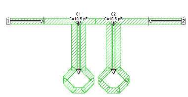
This is my (much simpler) implementations in an EM simulator of the general design as copied from the research paper, "Design of Fixed and Varactor-Tuned Bandstop Filters with Spurious Suppression_ A C Guyette_ ADA532920_ 2010".
[comment on this post] Append "/@say/your message here" to the URL in the location bar and hit enter.
I'm interested in solar radio astronomy. A lot of the radio emissions I am interested in span thousands of MHz. I also live downtown in a city next to a university with very powerful radio transmitters. In order to prevent those transmitters from interfering with my recordings I need to be able to filter them out. But most filters are only designed for narrow ranges of frequencies and have periodic bandstop harmonics (ie, stub filters) or stop working due to spurious modes at greater than 2x the bandstop frequency.
So I need a filter that can block ~5 MHz of bandwidth around 461 MHz but also pass signals (without attenuating them) all the way up to ~2000 MHz (4x the notch frequency). This design is suited particularly well for my use. I don't need tons of attenuation of the interfering radio signal. I just need to knock it down enough to stop it from causing problems but also pass everything else.
The resonant frequency is determined by the electrical length of the two parts of the resonator. The fat and the skinny parts (capacitor-like and inductor-like). The notch is at the frequency where the length of both combined equal 1/4 wavelength long. In theory.
But in my testing I also just completely removed the fat top part and replaced it with a discrete capacitor. With a value of ~10.5 pF I achieved the same bandstop frequency and depth as using the fat trace which had distributed capacitance. But this throws away the 3rd order spurious suppression *and* even changing the discrete cap's capacitance by 0.2 pF could shift the resonance 10 MHz. It'd be very fiddly. That's why in the paper they used varactors which could be tuned with voltage to adjust the capacitance.
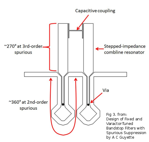
A C Guyette's design is based on a combination of two clever things. It takes a normal combline filter but then wraps around the coupling section twice, a dual-coupled-resonator in the lingo, which has some particular advantages. But the point of the paper, the really clever thing, is the integration of the delay lines and the coupling sections into the same structure and then being able to set the phase arbitrarily so each section constructively interferes.
The procedure to calculate the lengths require is very complex. I could not understand it. So in my design I don't even think the 2nd or 3rd order spurious modes are suppressed. But this particular dual-coupled combline resonator arrangement is still useful because it doesn't have strong harmonics at 2,3,etc times the notch bandstop frequency.
The resonator is composed or two PCB trace sections: the fat, capacitor like span and skinny, inductor like span are chosen to be 1/2 and 1/4 wavelength long respectively at the frequency of the 3rd spurious mode.
The microstrip length (between discrete resonators) is chosen to be 1 wavelength (360 deg) at the 2nd spurious mode frequency.
Together these two particular arrangements give rise to constructive interference at their respective spurious frequencies and mitigate them allowing the upper passband to be lower loss and extend further.
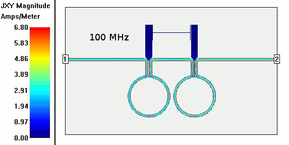
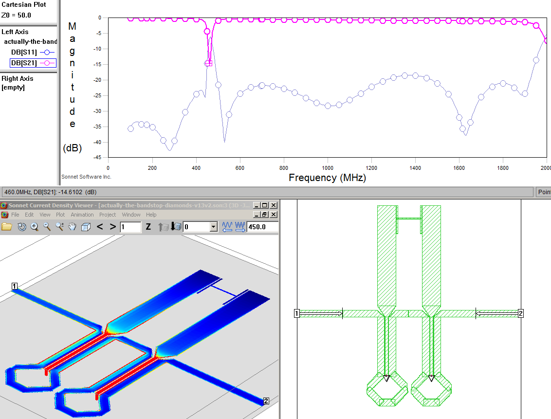
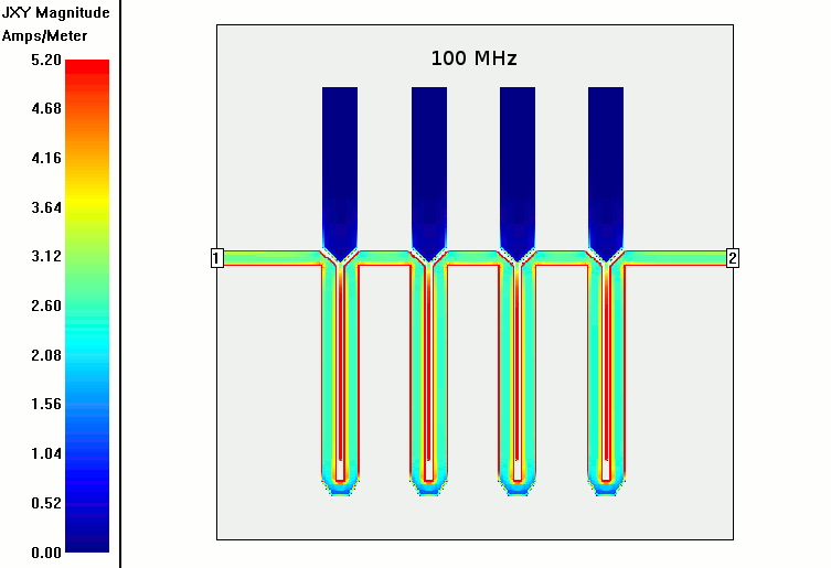
In the animation at the top of the current density over the microstrip and resonator elements from 100-2000 MHz the current flows mostly unmolested until about 1400 MHz when some insertion loss (~3dB) begins. That's about 2.3x the notch freq which probably means spurious modes not not being properly suppressed by the phase shift of the circle delay lines. I saw this behavior in most of the intertions I simulated for 461 MHZ.
All of these lengths are *electrical length* on the microstrip. For a FR4 board with assumed dielectric constant of 4.4 this means the scaling factor is 3.2 and not 4.4. I'm using http://leleivre.com/rf_microstrip.html to calculate this.
The lengths of the two resonators are inductively coupled together and destructively interfere at the frequency of of the stop band. Additional capacitance is added to this system by the thin H-shaped conductor capacitively coupling them.
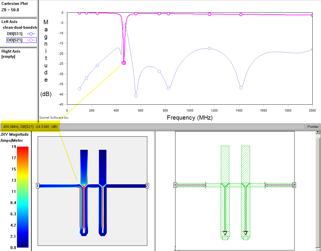
After making a series (~30+) of slightly (or drastically) changed versions of this type of filter in Sonnet I eventually converged on something that worked and could be simulated fairly quickly. I found out fast that it's helpful to avoid curves and having lots of excess transmission line. The end result of all these simulations were two different kinds of plots as shown below in for final version.
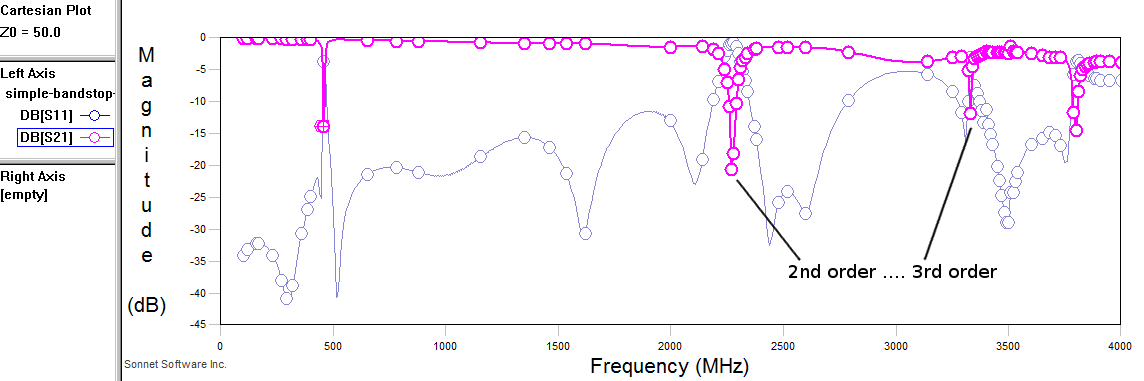
The point of the simulations is to generate scattering parameters for some set of conductors: what happens to the energy from one place to another on the circuit(s). This is typically shortened to S-Parameters and more usually just the notation like: S11, S12, and S21, etc. The left number S[1]2 is the direction the power goes to while the right S1[2] is where the power comes from. So S11 is the power reflected back to place 1 from place 1, S21 is the power going through from place 1 to place 2.
In the top chart S11, the return loss represents the amount of reflection back from the filter. The lower the amount of reflection back the more you can assume goes out and through. But S21 not S11 is what is (primarily) cared about in filters. It's the power received at port 2 from port 1. The dip in the pink S21 line represents stuff filtered out or lost due to other things. The lower the S21 at the bandstop frequency the better. But S11 has to be kept low (that is, minimal reflections) for all other frequency ranges otherwise there will be high loses for the stuff you want to pass through.
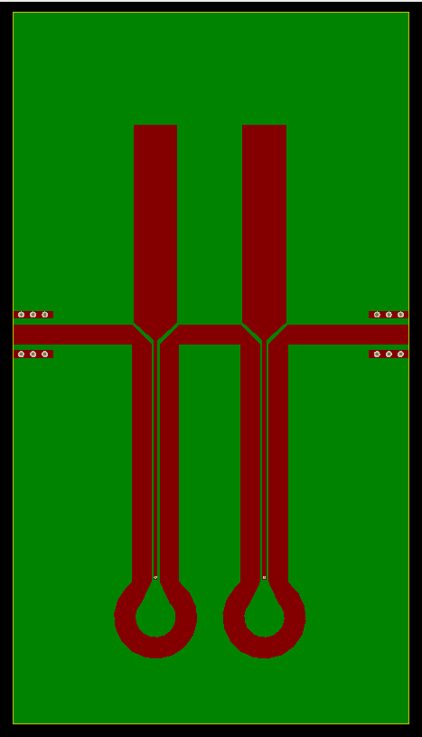
In the bottom left chart current density at a frequency near the bandstop is shown. It shows how lots of energy is coupled into the resonators and dumped to ground.
The bottom right shows the top-down view of the top copper metal layer. The width is 80mm and the height (not shown fully) is 100mm. The entire simulation is run assuming a metal box encasing it that is 80*100*10mm in volume.
After about a week of trying lots of different PCB filter techniques and topologies I had a much better handle on which aspects of the filters I needed for my requirements and how to use Sonnet to make them. So I went back and re-did the filter implementation from scratch and it turned out about -10 dB better than my first with the same number (2) of dual-coupled resonator sections! Nice. I then tried 4 resonator sections but the insertion loss for that path length was just a bit too much. 3, on the otherhand, was just right. So it was time to move on to kicad (again).
Since I had a good no frills version working and sent off to be fabricated I decided it was time to revisit the bottom delay line loops. Initially I had kind of just copied these without reason. I wasn't sure exactly how much the microstrip counted as part of it or exactly how to calculate the required length.
But after lots of testing and re-reading the paper and it's references and citations I finally got a hang of it, or so I thought. I could see my 2nd order spurious mode started at about 2500 MHz. Above what I needed but still, why not try to eliminate it? So I figured out i needed 118mm of path length but only have 87; 32mm needed. So I'd add a loop of ~4 * 8mm elements or something close. Of course while doing this I completely forgot that the electrical scale length would be 3.2 times less for FR4 of 4.4 dielectric constant. But the sim was already going.
It sort of helped the spurious mode but not a lot. And the close I got to 118m the worse it go. But what *did* change is the notch depth, for some reason. Whereas before with the simple, no-frills version I needed 3 resonator elements to get down to -35dB at 461 MHz now I could hit -37 dB with just *2* elements.
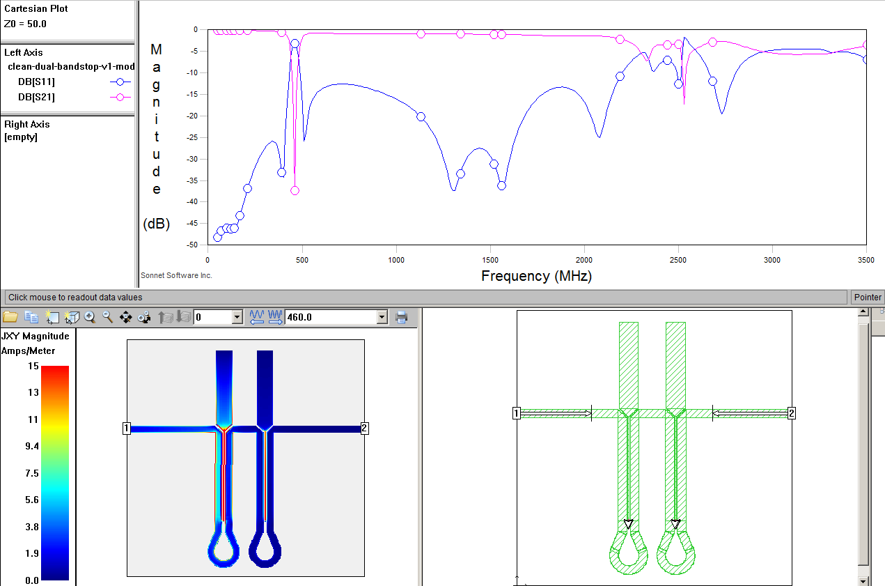
I don't know why, it's still cargo cult, but I like the results!
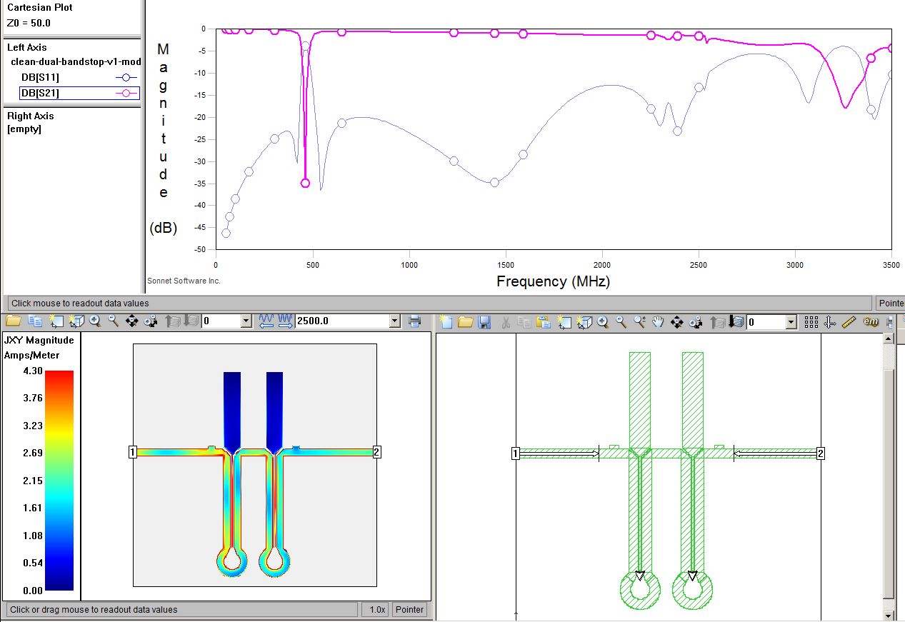
Another technique I had read about for mitigating high frequency supurious resonances was the use of small bumps (impedance discontinuities) on the microstrip that high frequencies around the spurious modes would 'see' and be interrupted by but lower freqs would pass on by. I kind of of just guessed at the scale needed and placement but with good results. In the example below you can see while I didn't wipe out the 2500 MHz second order spurious mode I did disrupt it quite a bit. With this technique the acceptable insertion loss upper passband could be extended another 500 MHz from 2 GHz. Not a trivial amount.
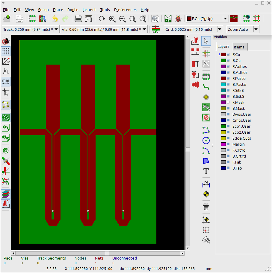
Make sure to draw in an explicit metallization rectangle on the GND layer instead of relying on the box GND. This means there'll be a green dashed rectangle outline when viewing the top metallization layer. Then export the gerbers, open in kicad with *GERBVIEW* then use gerbview's "Export to pcbnew" feature to save as a .kicad_pcb file, specifically $projectname.kicad_pcb and overwrite the auto-created one.
During the process gerbview will ask which layers are F.cu (front copper) B.cu (back copper) and so on. gerbview color codes this and you can toggle the layers on and off to see which is which.
You may notice the metal layer is rough and jagged with notches and mismatched bits in my first attempt shown below. In Sonnet there is a trade-off between grid cell size and computation time. While a 0.25 mm grid may take 10 minutes to sim a 0.1 mm grid will take half a day. The trick is to do the simulation at a large grid size, save that version then switch to a much smaller grid size, fix all the little jaggies and notches and mismatches, and export the gerber. Then save that small grid size version of the file as your gerber-out version and reload the original large grid version to continue work. It also helps if you pick a grid size that lends itself to even divisions when you're working. 0.25mm is my favorite.
Also very important in getting good gerbers out is to avoid using the centering tool, either horizontally or vertically, because it will place your objects offset from the grid and cause quantitization errors and irregularities due to not fitting the grid anymore.
Another hint that may be obvious to other people but wasn't to me was that the solder mask layers don't define where the solder mask *is*. Instead they define the holes where the solder mask *isn't*. I had quite a bit of trouble with this went first attempting to order PCB and kind of made myself look like an idiot.
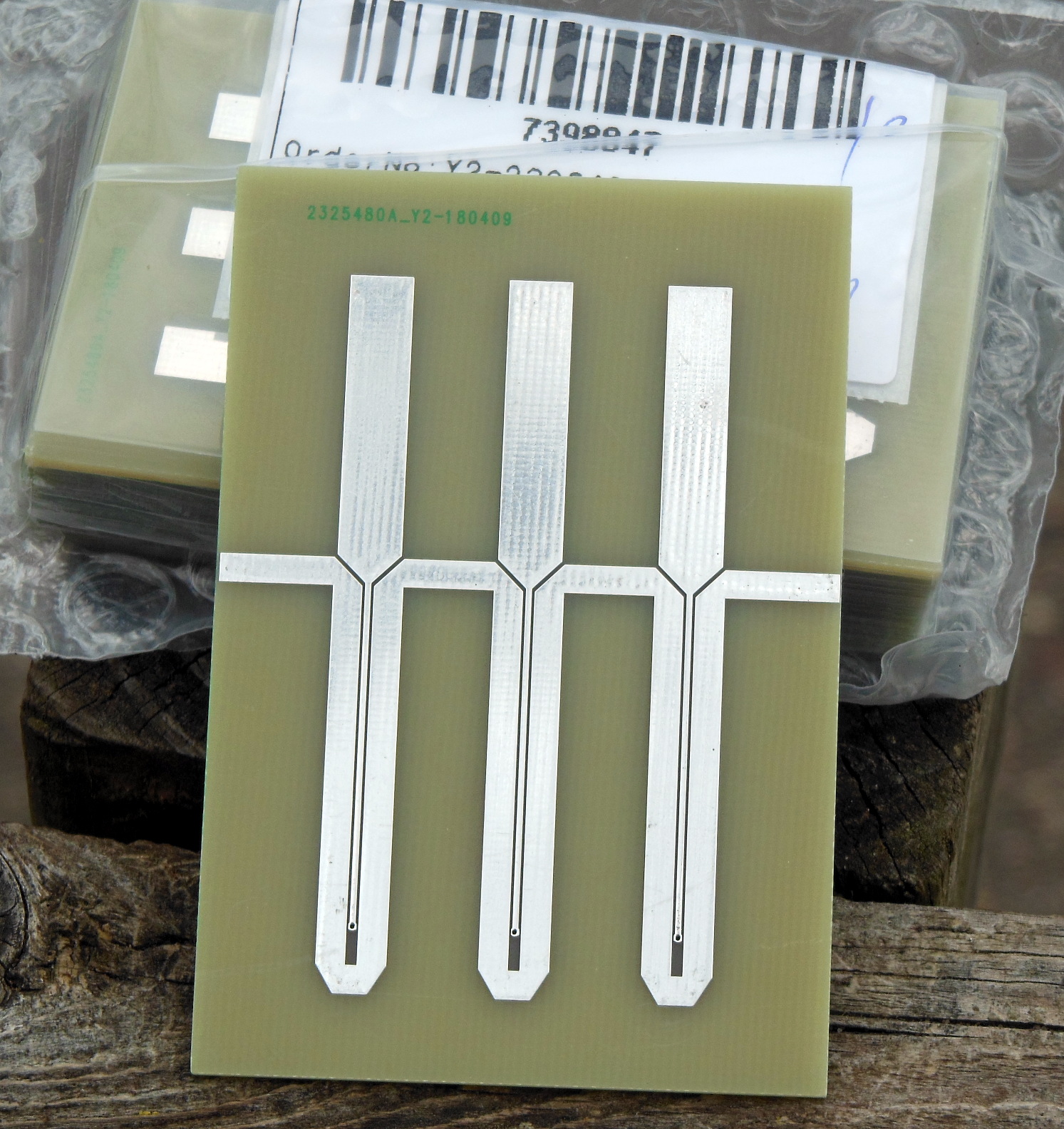
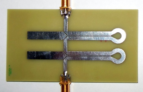
Final dimensions ended up 80mm*54mm*1.6mm.
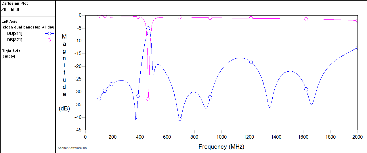
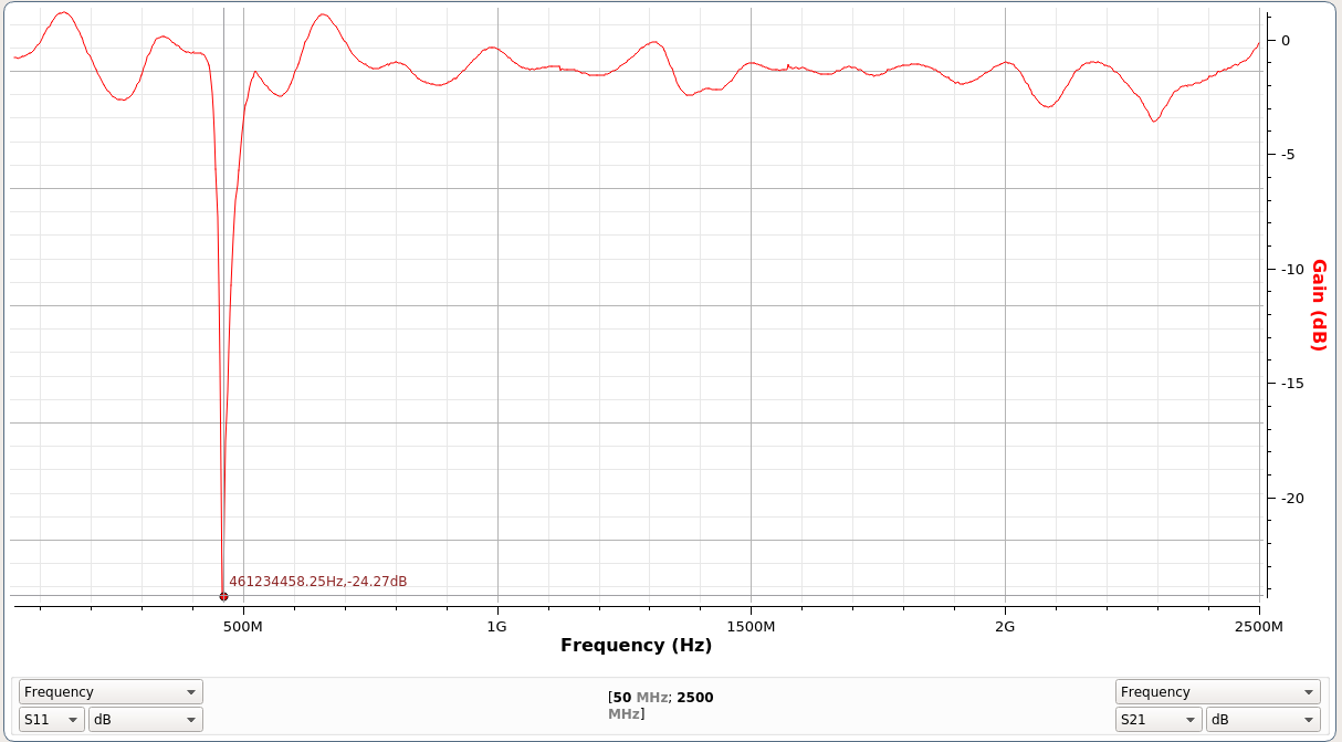
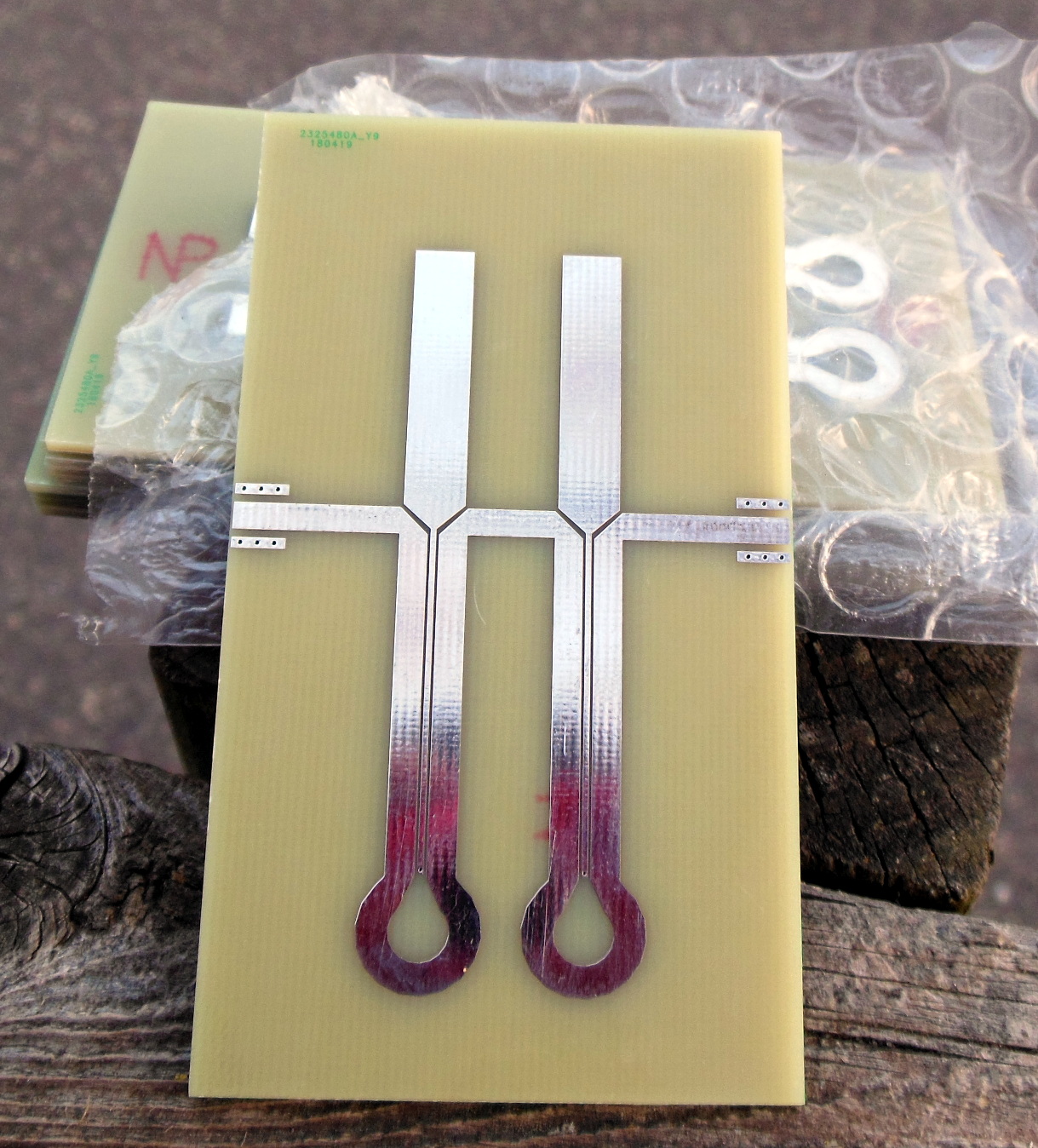
I made these improvements after I had already ordered the above fabricated. It achieves -35 dB insertion loss over 460-465 MHz with only two resonator elements. The improvement is entirely from the loop at the bottom. Not in the delay line sense but in the decoupling the two sides sense. Here it is in kicad with SMA end-launch fittings,
And here's the first VNA test. The frequency response is almost perfect. When I put it in the metal box, 1cm gap above, 1cm gap below, it should get even better.