Home: Planar PCB Radio Filters
 (2025-09-24: new code)
I've done open loop bandpass filters before but my prior design had no way to tune anything. It was just one band per design.
This is my attempt to implement a tunable radio frequency bandpass filter based off a paper I read. It uses planar PCB resonators that are tuned by a "digitally tunable capacitor" IC controlled by an esp8266 microcontroller.
I'm basically implementing the paper, "A UHF Third Order 5-bit Digital Tunable Bandpass Filter Based on Mixed Coupled Open Ring Resonators" by Ming-Ye Fu, Qian-Yin Xiang, Dan Zhang, Deng-Yao Tian, and Quan-Yuan Feng. But I translated the intent of the design from 0.8mm expensive (Er 2.65) PCB material to cheap 1.6mm thick FR4 PCB (Er 4.4) and I'm rolling my own microcontroller setup since theirs is not described.
[comment on this post] Append "/@say/your message here" to the URL in the location bar and hit enter.
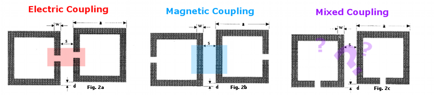
In open loop resonators very close to each other the type of coupling, either electric of magnetic, is a function of the location on the loop(s). At resonance the maximum electrical field density is across the gap and the maximum magnetic field density at the opposite side. So for magnetic coupling they are put "back" to "back" and for electric "face" to "face". By turning them so neither the max electric nor max magnetic field densities are close to the other the contribution of electric and magnetic coupling is about the same. The balance can also be altered by displacing them out of alignment. This is called mixed coupling.
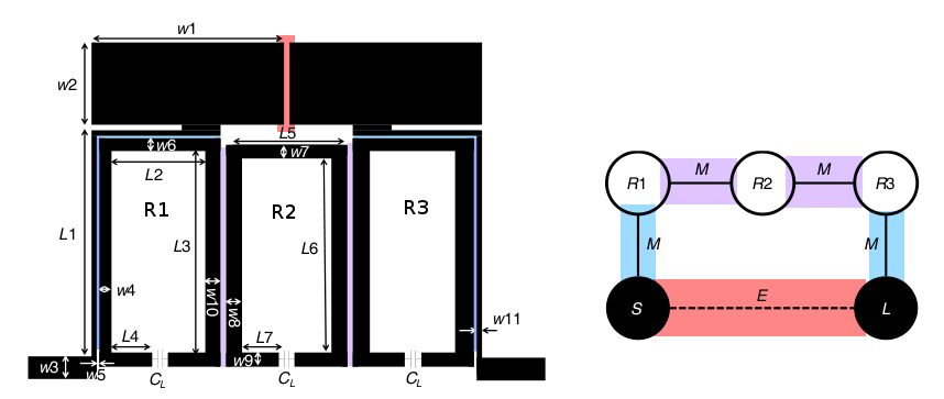
In this particular design RF energy takes two paths using the same start.
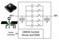
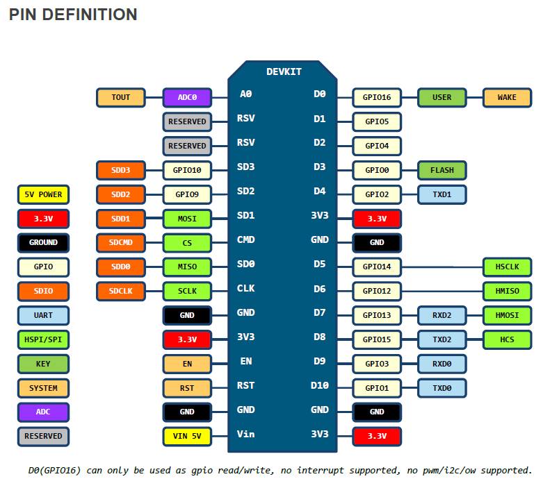
The tunability comes from using some really neat Peregrine Semiconductor IC called the PE64904; a "Digitally Tunable Capacitor" that works from 100-3000 MHz and spans 0.6 to 4.6 pF. This IC is put in the open end of the open ring resonators to tune them. It is controlled over the 3-wire SPI protocol which necessitates a microcontroller of some sort. I've chosen to use the cheap esp8266 series esp12e boards (~$5) because they come with wifi and I already have experience with them.
The commands it takes are very simple. You pull the chip select (CS) line low then send a message containing a hex number from 0 to 31 and return the CS high.
You may be thinking, "Why not use varactors instead? Then you don't need a computer you just need a variable voltage. It's much simpler." And it is in an absolute way. But the complexity of using a digital computer to control things is something I'm used to while designing a variable 0-30 voltage source that's precise and repeatable is not. And most importantly: the guys in the paper did it this way.
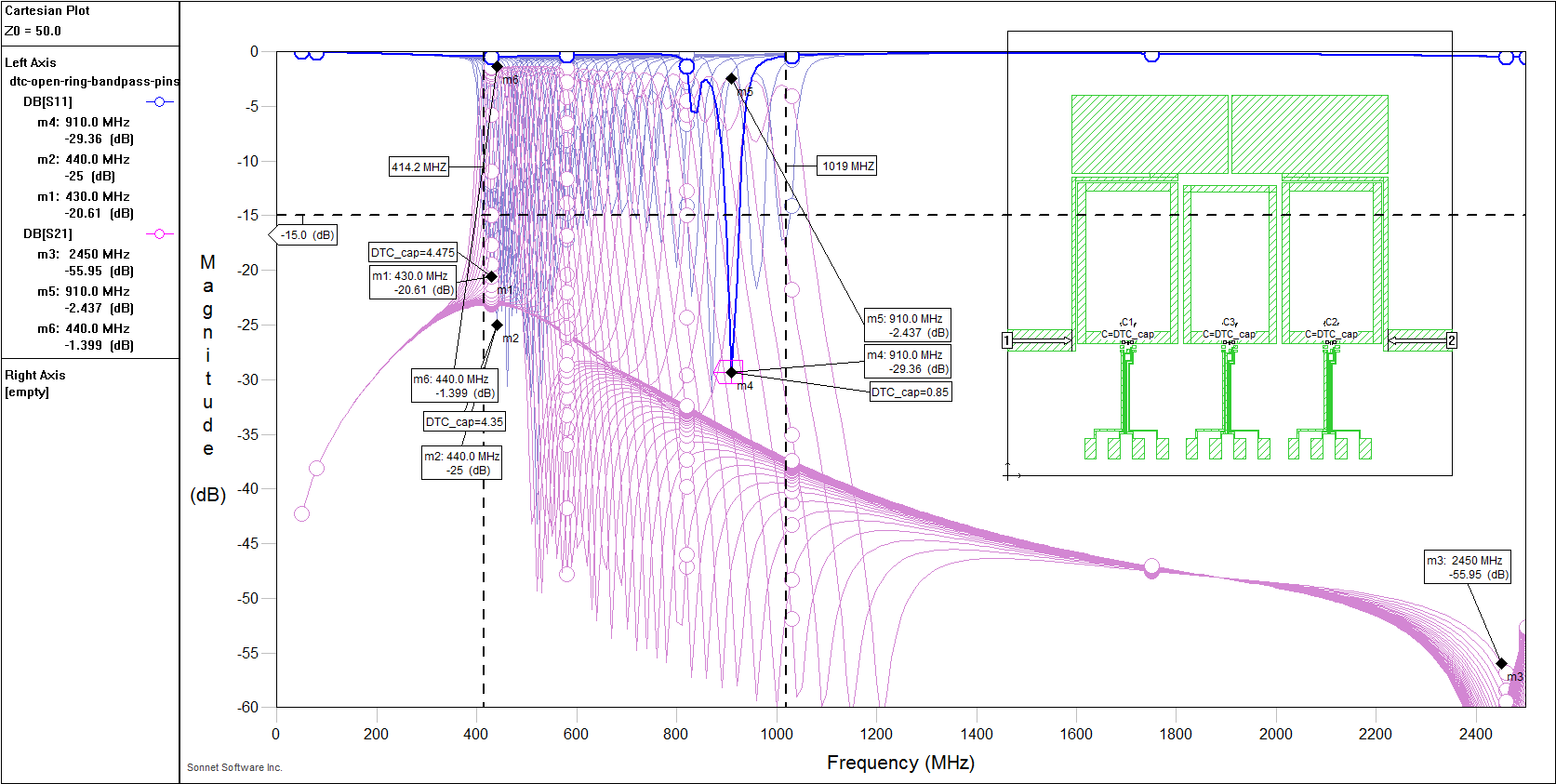
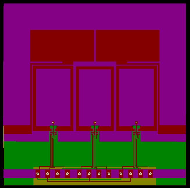
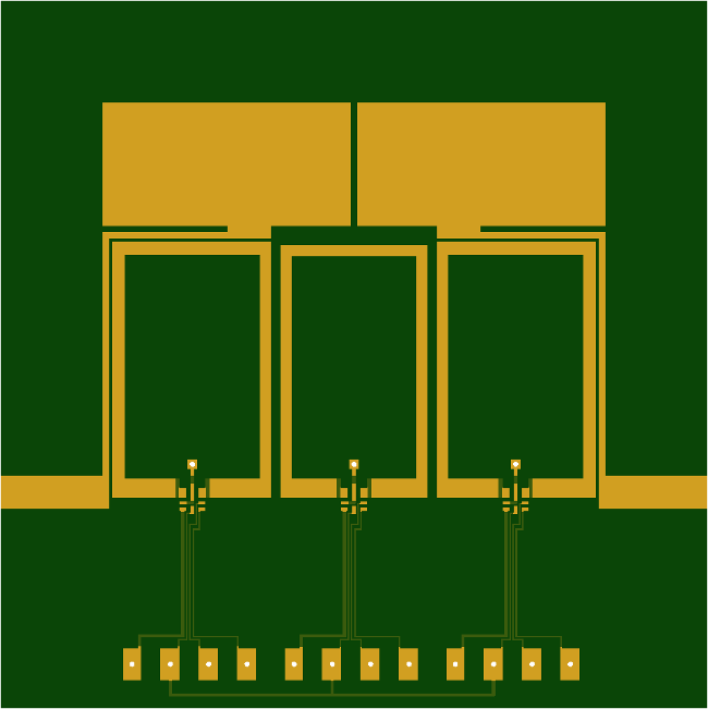
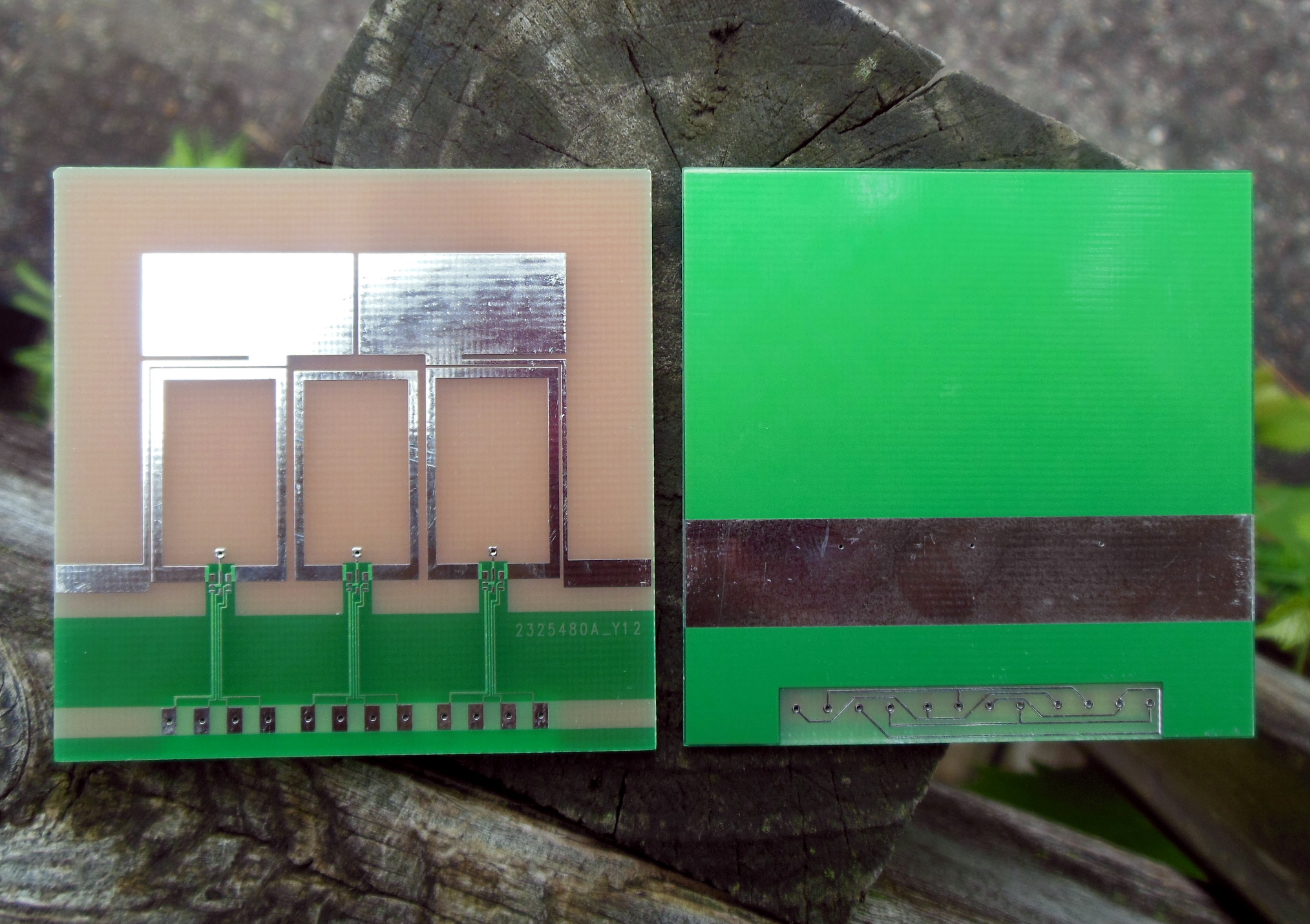
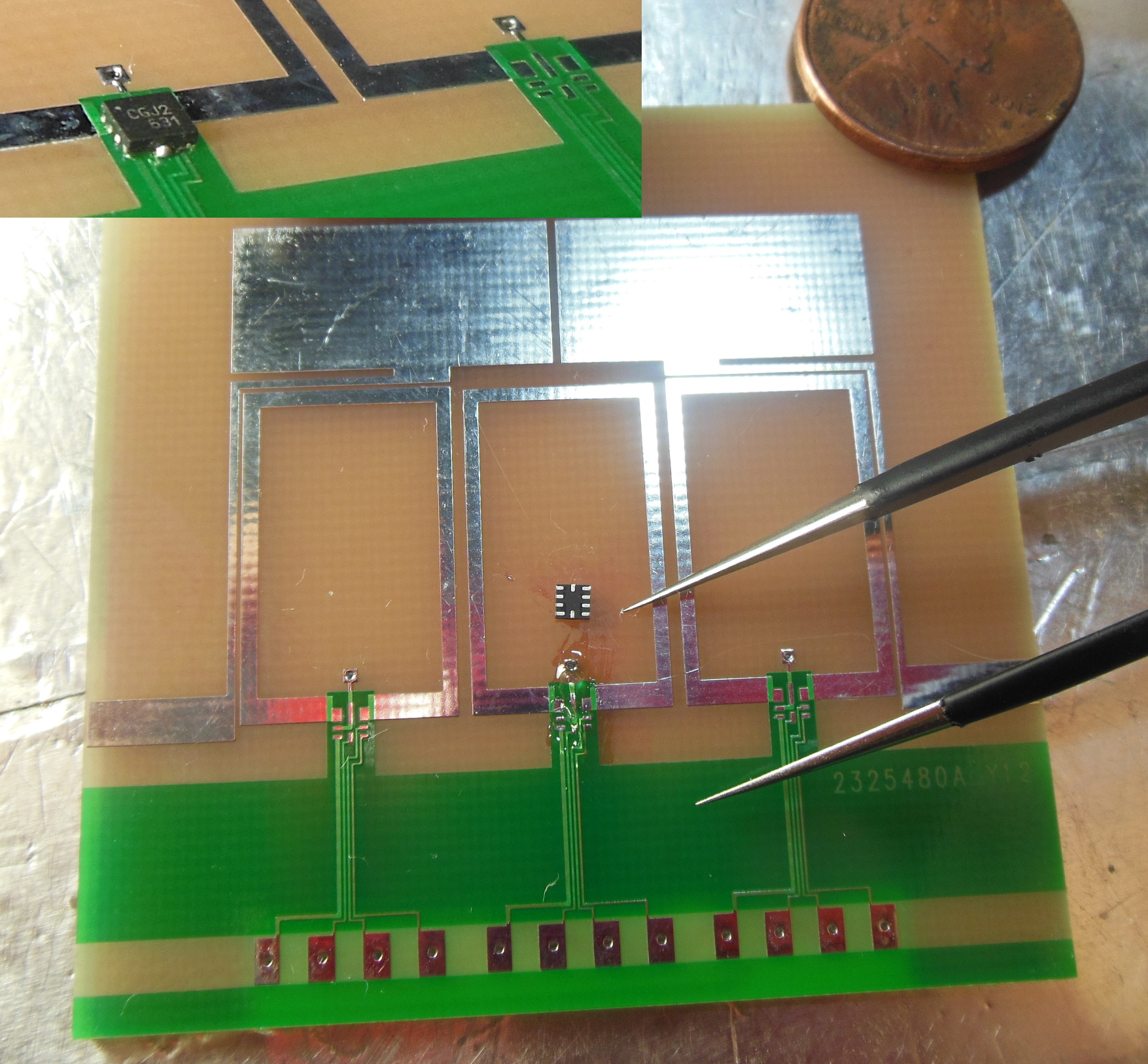
Below is the design as I implemented it on 1.6mm 4.4 dielectric FR4. For scale, the input port microstrip is 2.5mm wide (~55 Ohm). I compromised on a grid size of 0.125 mm and this led to a sim time of about 5 minutes (i5 3750K processor). The granularity of the grid to get this decent iteration time made directly copying dimensions infeasible even if they hadn't used 0.8 mm 2.65 dielectric F4B-2 substrate.
I ended up spending a bit of time using an online microstrip electrical length/phase calculator to translate the intent of the shapes to my different PCB material. And then a bit of fiddling back and forth with values when it didn't quite work.
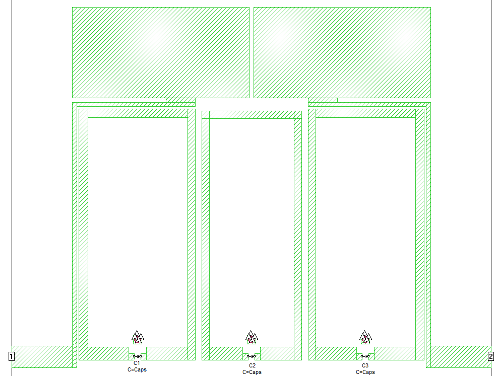
The little square pad with a via in it is for the PE64904 footpad ground. The two 0.75mm bits at the throat of the open loop are also to conform to the IC pads. I also tried adding the other IC footprint traces but the distance between them was very small and when I tried approximations with just one it didn't have much effect.
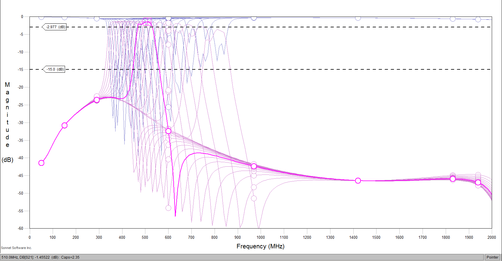
I set all the capacitors to the same variable, Caps, then did a parameter sweep of Caps from 0.6 to 4.6 mm at step size of 0.125 pF which is 32 steps and matches the PE64904 step size of 0.13 pF. Every other step is shown in the scattering parameters plot (0.25 pF step, 16 total).
The results matched the response reported in the paper pretty darn well.
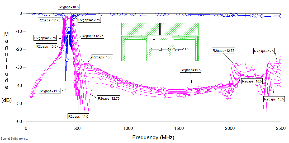
I ran some parameter sweeps of the various heights and gaps in the design to see what effected what.
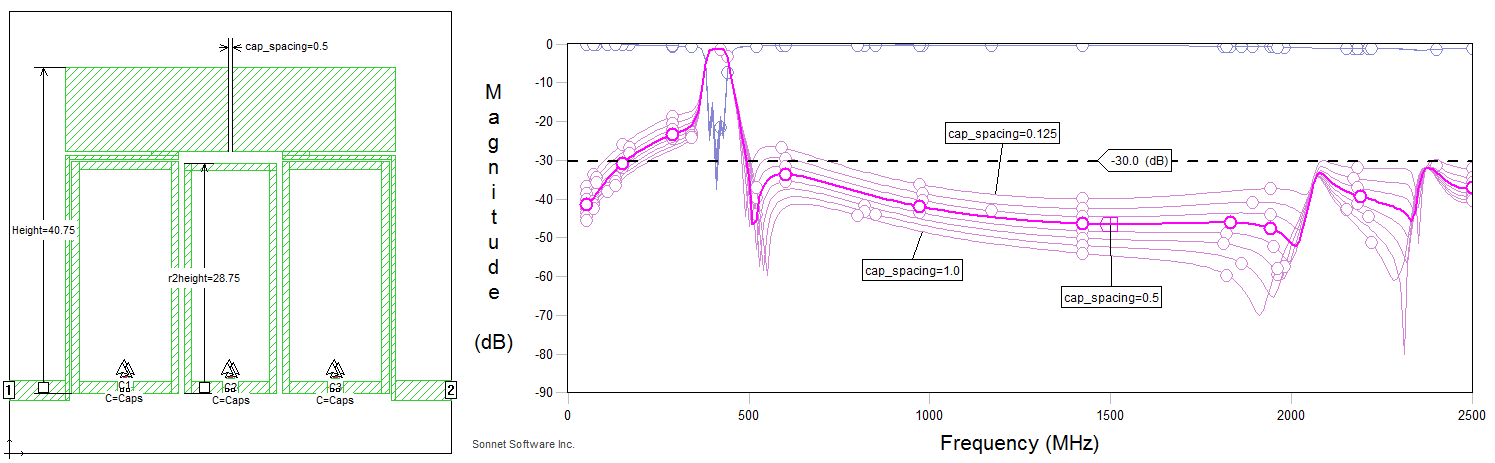
First I tried the spacing between the two capacitors up top. This did not effect the S11/return loss in any significant way. But it did have a significant effect on S21/insertion loss curves. Nominal spacing was 0.5mm and I covered 0.125 to 1 in 0.125 mm steps. With lower spacing (higher coupling) the 'zero' provided by destructive interference along this path shifted down in frequency towards the resonant freq. With higher spacing (lower coupling) the 'zero' moved up in frequency relative to the resonant freq. Over the parameter span the lower stopband insertion loss moved up and down by about 10 dB and the upper stopband by almost 20 dB in parts.
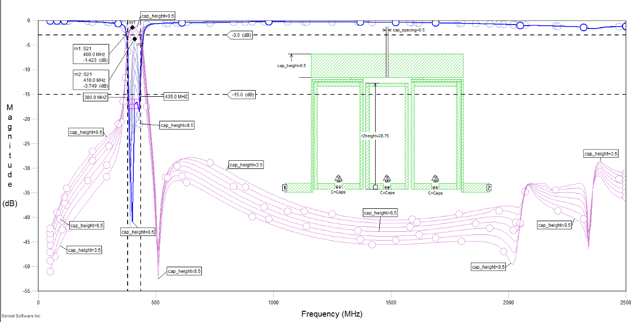
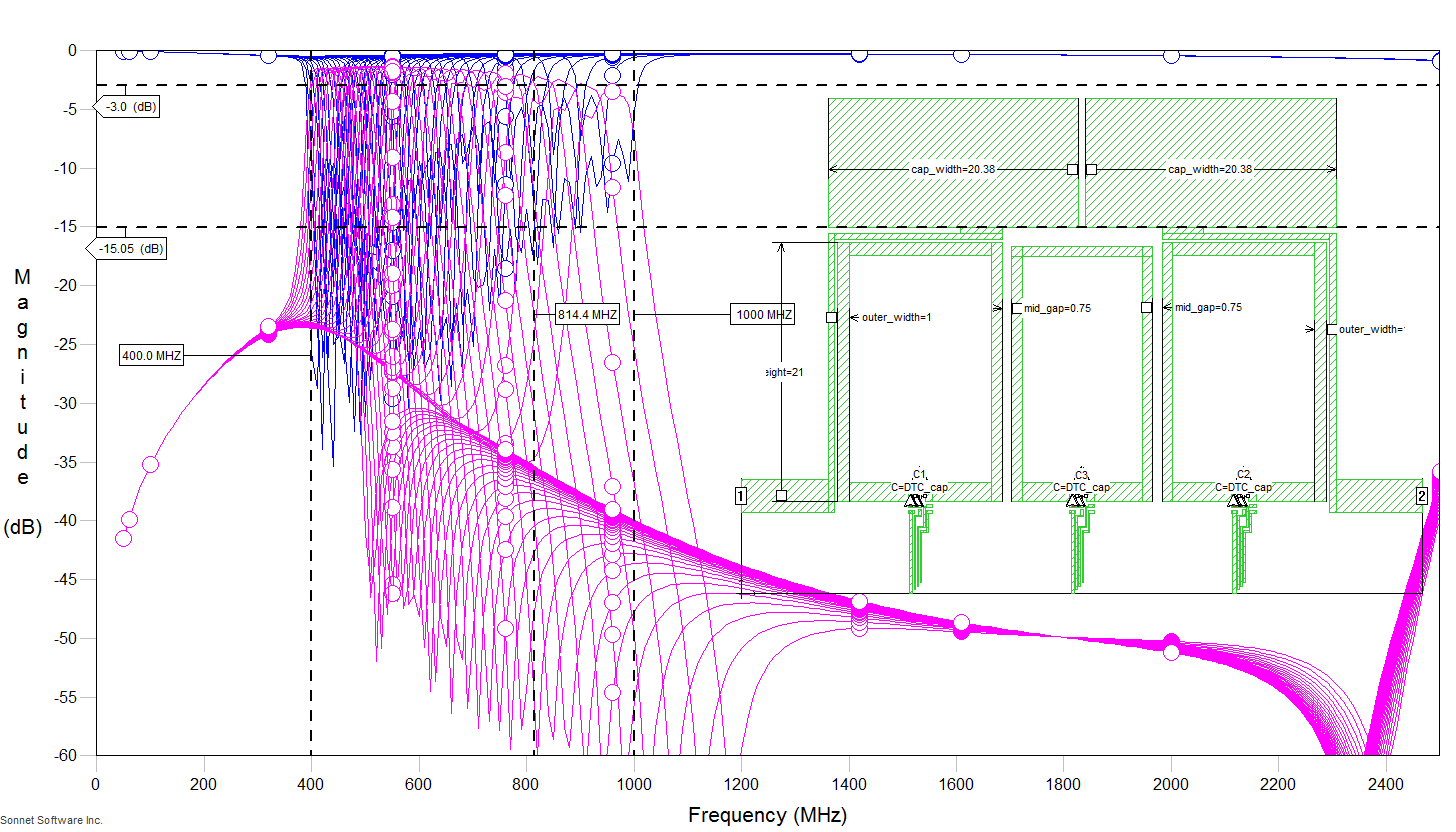
Optimal seems to be about 8.5-9.0 mm based on return loss (S11). The effect is less important on insertion loss (S21) but with increasing cap height (and so capacitance) the lower stopband drops off more slowly after -15dB down. With decreasing cap height the upper stopband pops back up higher after the high side zero but again only when it's already below -25 dB so not that important.
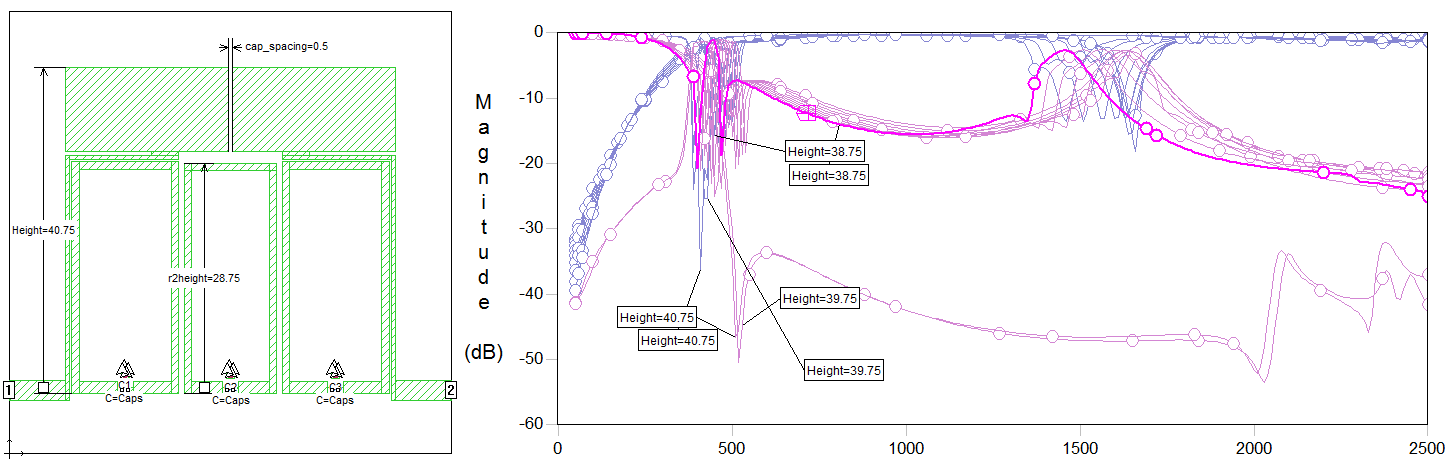
Then I tried altering the height of all the open loop resonators. This had a dramatic effect with a cliff in performance change after just a couple mm reduction in height. So resonator height/aspect ratio matters *a* lot. To be clear, the "height" parameter moved all the tops of the loops, the caps, and the coupling lines together. It kept their relative spacings exactly the same.
But maybe I did the scaling wrong and forgot to click some edge vertices or something. That would explain the sudden change if something began overlapping. I'll have to do this sweep again manually.
The results of shifting resonator 2's offset from the others was not very dramatic. There was little effect so I'm not going to put the plot up here.
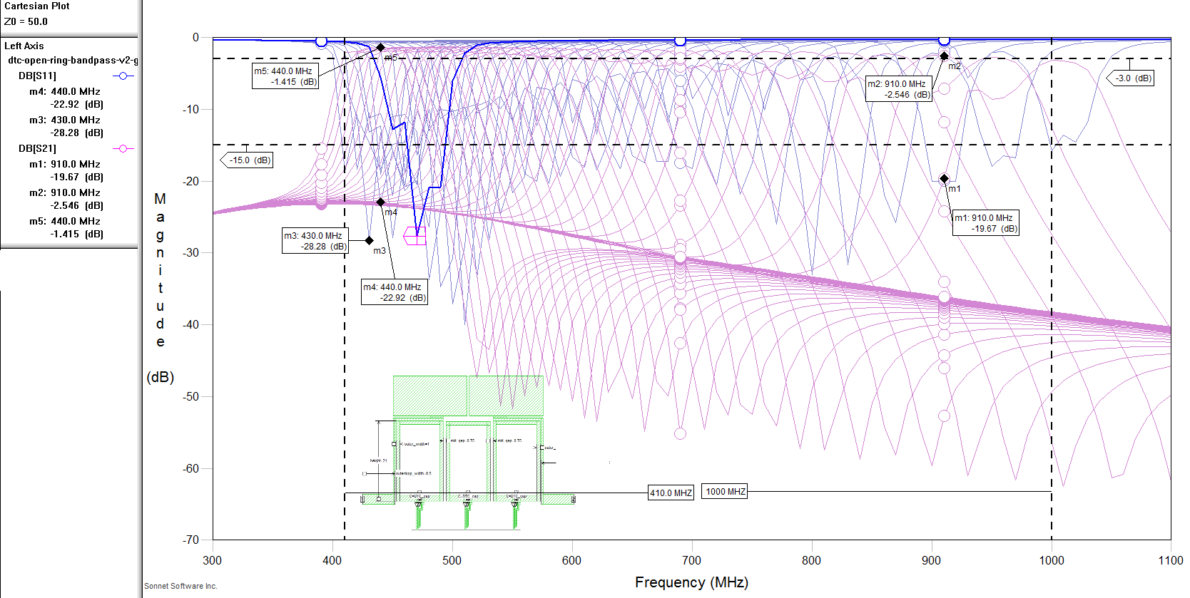
Some not so small tweaks in total height and coupling gaps eventually lead towards a version of the filter that would perform okay at 902-928 MHz. The total effective range is about 400 to 1000 MHz now but with some marginal performance on the high end (ie, -10dB S11 abd -3dB S21 for 915 MHz).
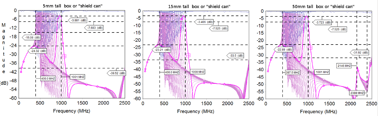
The large surface area shared between the metallic box and the PCB top metallization creates a significant paracitic capacitance. The closer the PCB metallization is to the conductive box ground the lower the impedance. This effect can be seen in the shift of the high frequency behavior of the transmission loss and in the decrease of the impedance of the microstrip ports from ~55 to ~52 Ohm.
It turns out I accidentally set a config preference to send vias up by default instead of down a layer or down to ground. That meant in a lot of the filters I designed recently were not completely realistic. So I had to go back and re-make them to tune them for performance with the proper vias and not some wire going 10mm up to the box walls.
It was actually easier to tune the open loop resonators with the vias going to the right place. I made a series of single parameter sweeps tweaking the line widths and gaps to see how the 3 dip peaks make up a single S11 notch moved. The balance of these was an S11 sweep with two resonances at either end of the tunable frequency range. At the high frequency end the contribution of one of the resonances is discarded to make the other two line up better.
The pass band is made asymmetric but this offsets for the increase relative bandwidth of the resonators with higher frequency. Instead only two peaks contribute and it's narrower but kind of shouldery and ugly. At the higher end this makes it so there are gaps between -15 to -15 db S11 passbands per DTC capacitance step.
The tradeoff is between having the small gaps in perfect passband coverage at the high end and the extended frequency range and better S11 the from overlaping only the 2 higher frequency dip peaks at higher frequencies. It'd be nice to get all 3 lined up at both low and high frequency ends but I can't figure that out.
The end result is pretty good, I think. It uses high 1cm box ceilings which I'll have to make myself out of tin rather than use an RF shield can. The final filter has a *simulated* range of 410-1000 MHz -15 db reflection loss and 1.5~3.25 dB insertion loss over that span.
The arrows on the vias now point down.
This lua code connects to to a hard coded wifi ssid then once it has an IP it connects to a TCP server running on a hardcoded IP and port. From there it waits for text instructions. On receiving anything in the form of a number from 0 to 31 it converts it to hex and sends it out the configured HSPI port to the digitally tunable capacitor.
Normally GPIO15 (pin D8) is used as a SPI 'Chip Select' line. But this requires adding external resistors in order to not trigger some boot issue. Additionally people on the forums have reported HSPI CS not working with NodeMCU. So since the PE64904 only requires 3 wires I instead disable the HSPI CS (GPIO15/D8) and the HSPI MOSI (GPIO13/D7) by setting their mode back to normal GPIO. Then I use the HSPI MOSI pin as a GPIO and manually pull it low as a chip select command before spi.send() then manually set it high after.
For a server on the computer it connects to I use use netcat like,
nc -l 6005
and then type, say, 15 and hit enter. If it works it responds "ok".
15
ok
-- esp8266 mediated wifi:telnet control of PE64904 SPI based digitally tuned capacitor.

-- Config				esp12e		PE64904
-- -- Default HSPI for CLK and MISO
-- local CLK = 5           	 --> GPIO14 D5 | MISO, PIN 7 (SDA)
-- local MISO = 6            	 --> GPIO12 D6 | SCL,  PIN 5 (SCL)
-- -- Manual CS/SEN for chip select
local CS = 7              	 --> GPIO13 D7 | SEN,  PIN 6 (SEN)
local duration = 3000     --> 3 seconds
local i = 0
local result = 0

-- Turn on HSPI (dev 1) SPI at (80 MHz/8) 10 MHz
spi.setup(1, spi.MASTER, spi.CPOL_LOW, spi.CPHA_LOW, 8, 8)

-- Manual CS Pin (instead of HSPI CS)
gpio.mode(CS, gpio.OUTPUT)
gpio.write(CS, gpio.HIGH)

-- Need to disable HSPI CS D8/GPIO15 from being toggled.
-- Set pull-up to prevent potential issues.
-- ref: https://nodemcu.readthedocs.io/en/master/en/modules/spi/#spisetup
gpio.mode(8, gpio.INPUT, gpio.PULLUP)

function string.fromhex(str)
	return (str:gsub('..', function (cc)
		return string.char(tonumber(cc, 16))
	end))
end
function string.tohex(str)
	return (str:gsub('.', function (c)
		return string.format('%02X', string.byte(c))
	end))
end

-- Connect to wifi
print(wifi.sta.getip())
wifi.setmode(wifi.STATION)
wifi.sta.config("ssid","password")
print(wifi.sta.getip())

-- Connect to control server
local flagClientTcpConnected=false;
print("Start TCP Client");
tmr.alarm(3, 5000, 1, function()
	if flagClientTcpConnected==false then
		print("Trying to connect to server");
		local conn=net.createConnection(net.TCP, false)
		conn:connect(6005,"192.168.1.125");
		conn:on("connection",function(c)
			print("TCPClient:connected to server");
			flagClientTcpConnected = true;
		end)
		conn:on("disconnection",function(c)
			flagClientTcpConnected = false;
			conn=nil;
			collectgarbage();
        	end)
		conn:on("receive", function(conn, m)
			print("TCPClient:"..m);
			for i = 0,31 do
				if string==i then
					hexval = i.tohex()
					gpio.write(CS, gpio.LOW)      -->Activate the SPI chip
              				tmr.delay(1)                  -->1us Delay
					wrote = spi.send(1,hexval)    -->Write hex value
					gpio.write(CS,gpio.HIGH)      -->De-activate the SPI chip
					print("Started SPI DTC Control");
					conn:send("ok\r\n");
					tmr.delay(100)
				end
			end
		end)
	end
end)
For the init.lua file I use one I cribbed from the DoitCar demo from www.doit.am bbs.doit.am. Change "spiviaweb-nogpio15-v1.lua" to whatever matches.
--DoitCar Ctronl Demo
--sta mode
--Created @ 2015/05/14 by Doit Studio
--Modified: null
--http://www.doit.am/
--http://www.smartarduino.com/
--http://szdoit.taobao.com/
--bbs: bbs.doit.am
--

print("\n")
print("ESP8266 Started")

local exefile="sta"
local luaFile = {exefile..".lua","spiviaweb-nogpio15-v1.lua"}
for i, f in ipairs(luaFile) do
	if file.open(f) then
      file.close()
      print("Compile File:"..f)
      node.compile(f)
	  print("Remove File:"..f)
      file.remove(f)
	end
 end

if file.open(exefile..".lc") then
	dofile(exefile..".lc")
else
	print(exefile..".lc not exist")
end
exefile=nil;luaFile = nil
collectgarbage()
So, I was having problems on the software side for a long time. It was sending and receiving to the esp but the PE64904 wasn't retuning or doing anything. Because my code sucks and is broken. But now it's the wild future of 2025 and I can just throw my bad code + nodemcu spi/PE64904 docs + esp8266 board quirks explanation at an LLM AI and debug working code into existence. Oviously time to revisit this project and finish what I couldn't alone.
And it's a good thing too. The nodemcu language itself, the esptool for flashing, and pretty much everything changed in the past 7 years that I've been doing nothing. None of the old code or toolchain worked with the new firmwares. Luckily AI helped figuring out why flashing wasn't working properly.
To flash the firmware get a modern (at least 2.x) version of esptool and a firmware with spi module and all the basic bits. You can use the one I had generated at https://nodemcu-build.com/: nodemcu-release-8-modules-2025-09-24-20-40-37-integer.bin if you want.
superkuh@janus:~/tests$ sudo esptool --port /dev/ttyUSB0 write_flash --flash_mode dio 0x00000 ~/blob/nodemcu-release-8-modules-2025-09-24-20-40-37-integer.bin
esptool.py v2.8
Serial port /dev/ttyUSB0
Connecting....
Detecting chip type... ESP8266
Chip is ESP8266EX
Features: WiFi
Crystal is 26MHz
MAC: 5c:cf:7f:0b:96:c5
Enabling default SPI flash mode...
Configuring flash size...
Auto-detected Flash size: 4MB
Erasing flash...
Flash params set to 0x0240
Took 2.63s to erase flash block
Wrote 450560 bytes at 0x00000000 in 50.5 seconds (71.4 kbit/s)...

Leaving...
Hard resetting via RTS pin...
After flashing the very user friendly java program ESPlorer can be used to upload/edit/compile/etc code on the esp8266. Baudrate 115200. Upload (and compile to .lc) the pe64904_controller.lua before the init.lua otherwise it'll get into a loop complaining about it not being there. Make sure to edit the IP address, ssid, and password in the init.lua.
-- esp8266 mediated wifi:telnet control of PE64904 SPI based digitally tuned capacitor.
-- Config esp12e PE64904
-- Default HSPI for CLK and MISO
-- local CLK = 5 --> GPIO14 D5 | MISO, PIN 7 (SDA)
-- local MISO = 6 --> GPIO12 D6 | SCL, PIN 5 (SCL)
-- Manual CS/SEN for chip select using GPIO13 (D7) instead of GPIO15 (D8)
-- IMPORTANT HARDWARE LIMITATION:
-- GPIO15 (D8) is normally HSPI CS, but ESP8266 requires GPIO15 LOW during boot
-- This creates a conflict - GPIO15 must be pulled low for boot, but SPI CS needs to toggle
-- Many NodeMCU users report HSPI CS (GPIO15) not working reliably
-- WORKAROUND: Use GPIO13 (HSPI MOSI) as manual CS, disable automatic HSPI CS
local CS = 7 --> GPIO13 D7 | Manual SEN/CS for PE64904 PIN 6 (SEN)

-- Turn on HSPI (dev 1) SPI at 10 MHz (80 MHz/8)
-- Only using CLK (GPIO14/D5) and MISO (GPIO12/D6) - MOSI not needed for PE64904
spi.setup(1, spi.MASTER, spi.CPOL_LOW, spi.CPHA_LOW, 8, 8)

-- Configure GPIO13 (D7) as manual CS instead of MOSI
gpio.mode(CS, gpio.OUTPUT)
gpio.write(CS, gpio.HIGH)  -- PE64904 SEN starts HIGH

-- Disable automatic HSPI CS on GPIO15 (D8) to prevent conflicts
-- GPIO15 needs pulldown for boot, but we're not using it for CS anyway
gpio.mode(8, gpio.INPUT, gpio.PULLUP)  -- Keep GPIO15 safe but unused

-- FIXED: Defined as a local function, not added to the string table
local function fromhex(str)
    return (str:gsub('..', function (cc)
        return string.char(tonumber(cc, 16))
    end))
end

-- FIXED: Defined as a local function, not added to the string table
local function tohex(str)
    return (str:gsub('.', function (c)
        return string.format('%02X', string.byte(c))
    end))
end

-- This part of the code is redundant because init.lua already connects to WiFi.
-- It's safe to leave it, but it's not actually being used when called from init.lua.
print("Controller script loaded. Last known IP: " .. wifi.sta.getip())

function start_tcp_client()
    local flagClientTcpConnected = false
    print("Start TCP Client")

    local timer = tmr.create()
    timer:alarm(5000, tmr.ALARM_AUTO, function()
        if not flagClientTcpConnected then
            print("Trying to connect to server")
            local conn = net.createConnection(net.TCP, false)
            conn:connect(6005, "192.168.1.125")

            conn:on("connection", function(c)
                print("TCPClient: connected to server")
                flagClientTcpConnected = true
            end)

            conn:on("disconnection", function(c)
                print("TCPClient: disconnected from server")
                flagClientTcpConnected = false
                conn = nil
                collectgarbage()
            end)

            conn:on("receive", function(c, payload)
                print("TCPClient received: " .. payload)
                -- Strip whitespace and extract number
                local cleaned = payload:gsub("%s+", "")
                local numval = tonumber(cleaned)

                if numval and numval >= 0 and numval <= 31 then
                    local spi_data = numval

                    gpio.write(CS, gpio.LOW)
                    tmr.delay(1)
                    gpio.write(CS, gpio.HIGH)
                    tmr.delay(1)

                    local bytes_sent = spi.send(1, spi_data)

                    tmr.delay(1)
                    gpio.write(CS, gpio.LOW)
                    tmr.delay(1)

                    print("SPI DTC Control sent state: " .. numval .. " (" .. bytes_sent .. " bytes)")
                    c:send("ok\r\n")
                else
                    print("Invalid value received: " .. tostring(payload))
                    c:send("error: value must be 0-31\r\n")
                end
            end)
        end
    end)
end

-- Start the main logic
start_tcp_client()
print("Ready to Set up wifi mode")
wifi.setmode(wifi.STATION)

-- Uses the modern table-based syntax
wifi.sta.config({ ssid="basestationame", pwd="password" })
wifi.sta.connect()

local cnt = 0

-- NEW TIMER API: Create a timer object first
local wifi_timer = tmr.create()

-- NEW TIMER API: Call the alarm method on the object
-- tmr.ALARM_AUTO makes it repeat automatically
wifi_timer:alarm(1000, tmr.ALARM_AUTO, function(t)
    if (wifi.sta.getip() == nil) and (cnt < 20) then
        print("Trying Connect to Router, Waiting...")
        cnt = cnt + 1
    else
        -- NEW TIMER API: unregister the timer to stop it.
        -- 't' is the timer object that is passed to the callback
        t:unregister()

        if (cnt < 20) then
            print("Config done, IP is "..wifi.sta.getip())
        else
            print("Wifi setup time more than 20s, Please verify config. Then re-download the file.")
        end
        cnt = nil
        collectgarbage()
        dofile("pe64904_controller.lc")
    end
end)
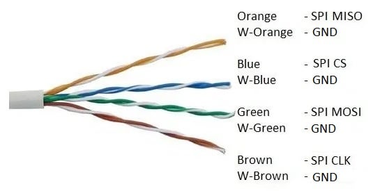
"The common method to wire shielded cables is to ground only the source end of the shield to avoid ground loops."
"If you do send single ended SPI over twisted pair cable, select one conductor of each twisted pair and make it a ground conductor. This way each signal line will have a pretty much equal electrical environment and you'll at least utilize the twisted pair to reject very high frequency magnetic interference. "
This system allows remote control of a PE64904 Digitally Tunable Capacitor via WiFi using an ESP8266 NodeMCU board. The capacitor can be tuned to 32 different states (0-31) for RF filter applications.
Computer -> TCP/IP -> ESP8266 -> SPI -> PE64904 -> RF Filter Tuning
nc -lvp 60050 -> Minimum capacitance (0.60 pF)15 -> Mid-range capacitance (~2.54 pF) 31 -> Maximum capacitance (4.60 pF)ok error: value must be 0-31Power On -> init.lua loads -> Compile pe64904_controller.lua -> Execute
What Happens:
init.luaSPI Setup -> GPIO Configuration -> WiFi Connection
Hardware Setup:
WiFi Connection:
WiFi Ready -> Connect to Server -> Wait for Commands
Network Setup:
192.168.1.125:6005 every 5 secondsWhen a command arrives:
Receive TCP Data -> Strip Whitespace -> Parse Number -> Validate Range
Validation Logic:
Prepare SPI Data -> Execute PE64904 Protocol -> Send Confirmation
PE64904 SPI Protocol Sequence:
SEN = LOW (idle state)SEN = HIGH (start transaction) SEN = LOW (falling edge latches data into PE64904)SPI Success -> Log State -> Send "ok" -> Wait for Next Command
SPI/Validation Failure -> Send Error -> Wait for Next Command
The system runs in an infinite loop:
$ (! 2004)-> nc -lvp 6005
Listening on [0.0.0.0] (family 0, port 6005)
Connection from [192.168.1.123] port 6005 [tcp/x11-5] accepted (family 2, sport 14967)
15
ok
99
error: value must be 0-31
ESP8266 PE64904 DTC Controller Started
Connected with IP: 192.168.1.123
Start TCP Client
TCPClient: connected to server
TCPClient received: 15
SPI DTC Control sent state: 15 (1 bytes)
TCPClient received: 99
Invalid value received: 99
The system is designed for robust, continuous operation suitable for remote RF filter tuning applications.