Home: Planar PCB Radio Filters
Latest Update: 2018-06-21
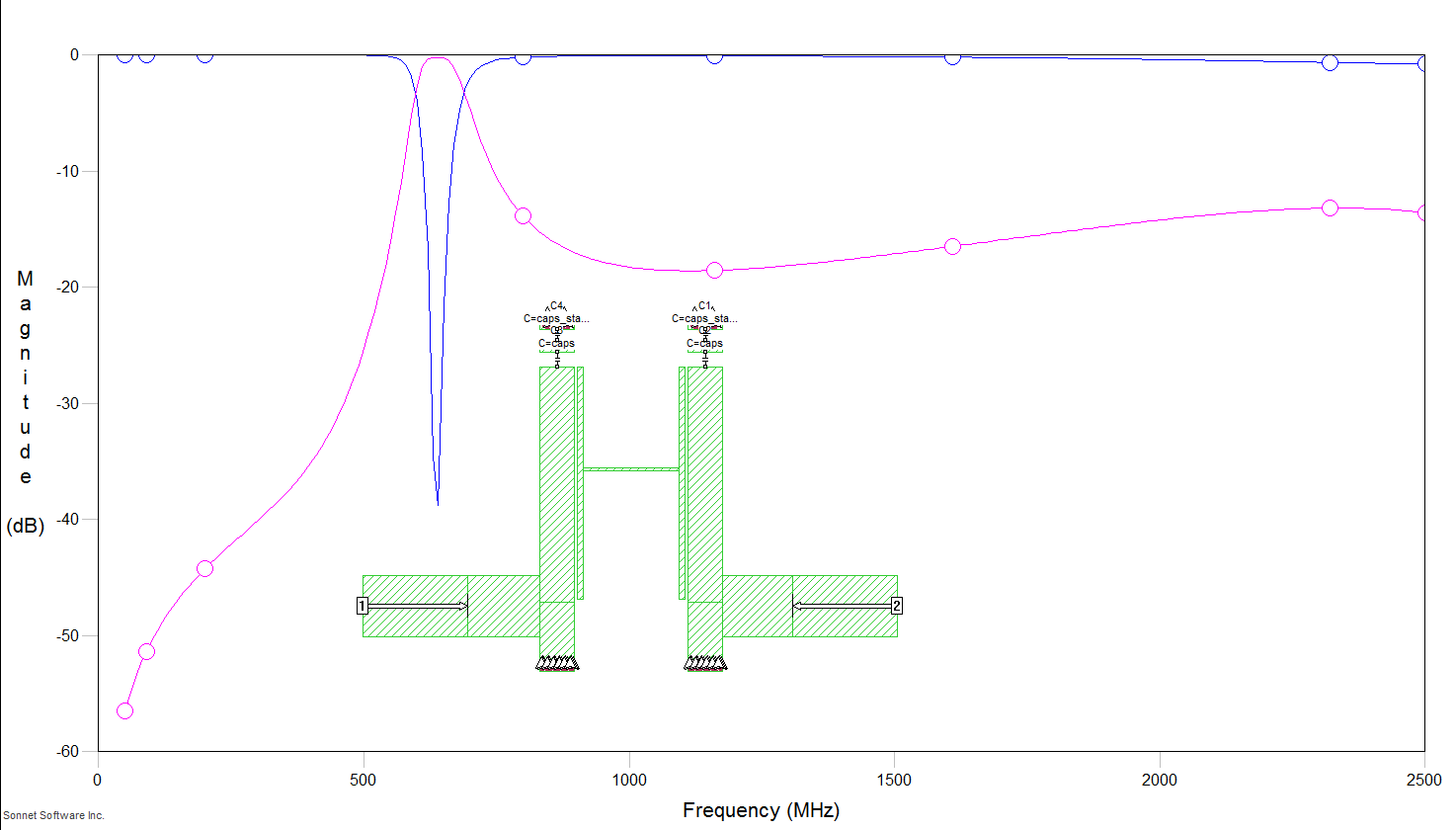
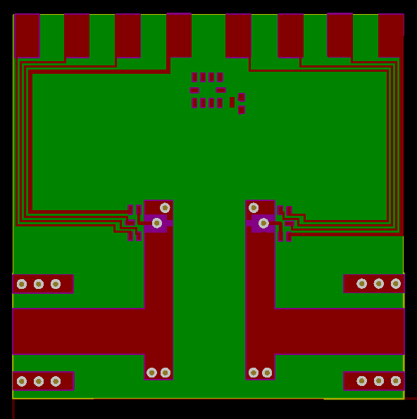
This is a planar implementation of the combline filter with 2 elements. Unlike coupled transmission lines the spacings in combline elements aren't absurdly precise. In this design the elements are ~4.5 mm apart but 0.25 mm either way makes little difference.
I'm implementing the design in "Tunable Tapped Combline Bandpass Filters for RFID Systems" by M. S. Siri, B. W. Schafer, A. M. Steffen, A. Eroglu and D. Ronnow except using 1.6mm FR4 dielectric. And instead of varactors I'm using 2*2mm digitally tuned capacitor ICs.
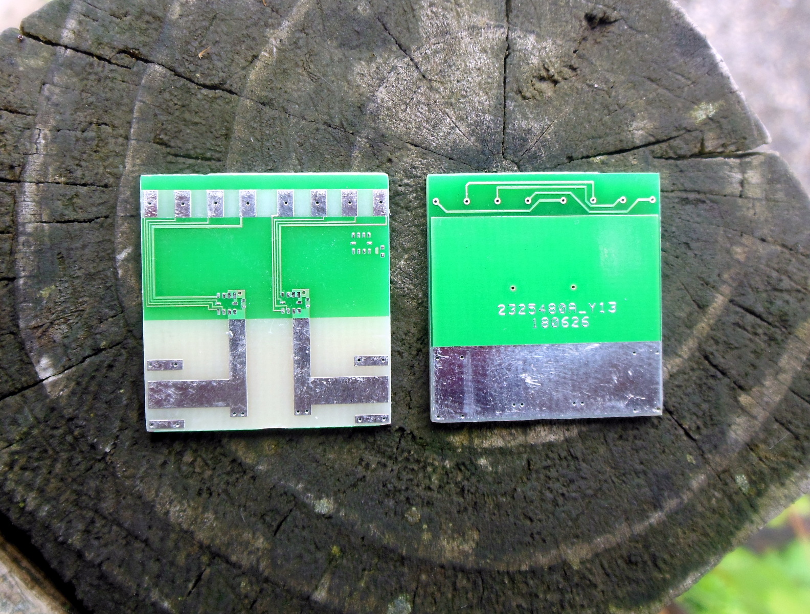
The entire thing is much tinier than it looks. It's problematically tiny with the final layout including pin headers being 23*29mm in size, slightly larger than a postage stamp.
[comment on this post] Append "/@say/your message here" to the URL in the location bar and hit enter.
After running a lot of parameter sweeps to figure out how it worked I settled on some fix spacings and lengths. The performance was decent, good insertion loss, but the upper stopband was marginal.
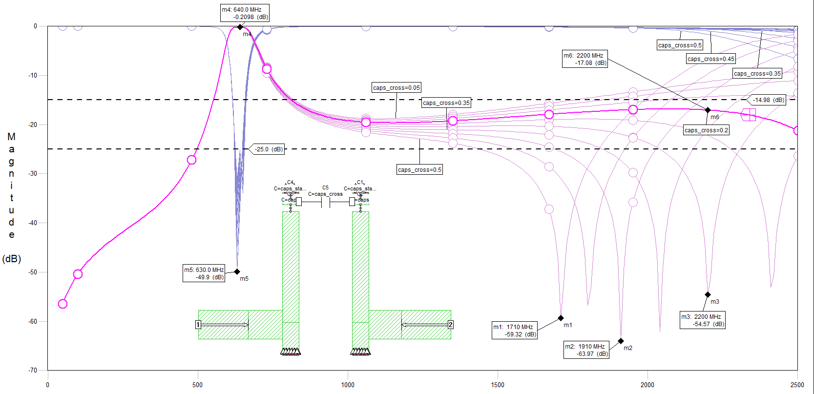
I decided to investigate adding electrical coupling between the two combline elements at one end. By changing the coupling from 0 to 0.5 pF the simulator suggests the zero can be pulled down from the higher frequencies to upside the passband just a moderate bit. But if it's pulled down too far the rebound after the zero becomes a problem.
A good balance seems to be 2.5-3 pF. That's well within the range that can be tuned by varactors or digitally tuned capacitors. The trouble comes in finding a way to actually put that capacitance in there without effecting other things. In practice I think I have to couple across the main combline elements rather than between the static and variable caps.
That arrangment is shown in the third plot. It was interesting to me that now the coupling effected the lower stopband as well. And it had an effect on S11 with large couplings (still good at 0.2 pF though). If I had a magic 4.875 mm 0.2 pF physical cap things would be fine.
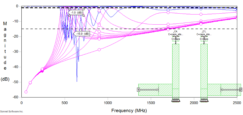
In order to get 1 to 2 pf I figured I'd need about 1cm of length. So I made a big H of conductor between the comblines. This seemed to work although it wasn't quite as much capacitance as I'd like. It still moves the zero down in freq a little bit and pulls the upper stopband down.
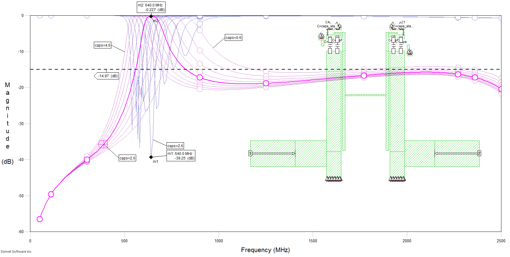
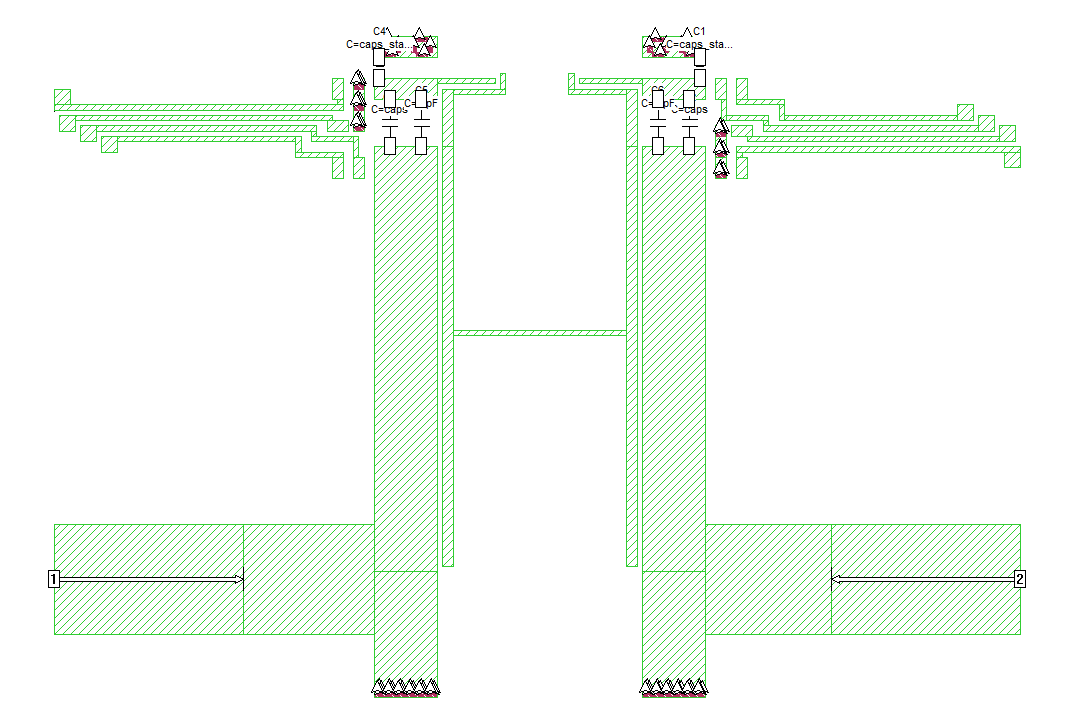
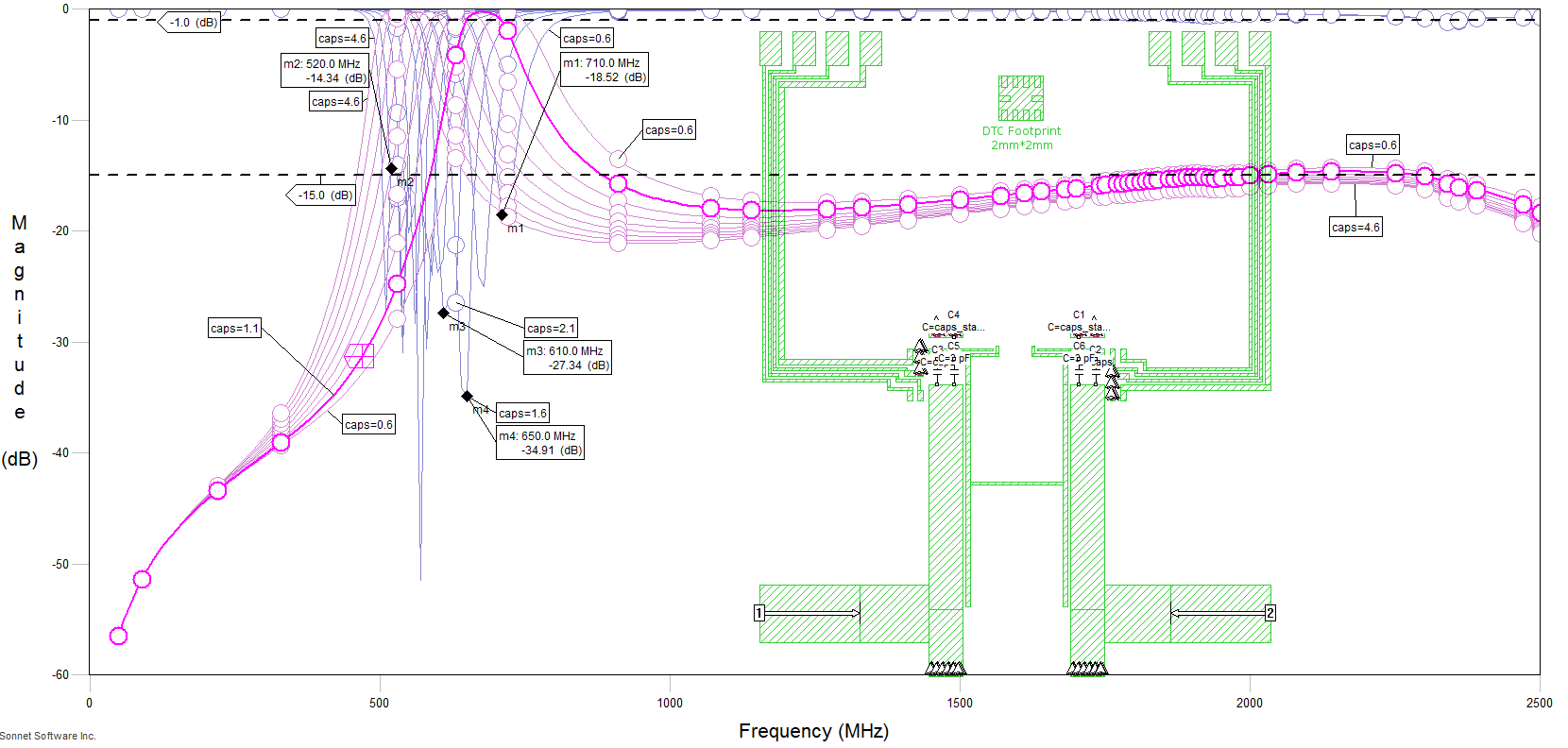
The Peregrine Semiconductor PE64904 "Digitally Tunable Capacitor" ICs are 2x2mm is size with 1x1mm area needed for the pairs of RF+ and RF- pads. I changed the top of the combline around a bit so that they would fit in. I also decided to add another static 3 pF cap in parallel with the DTC to help push things towards the useful tuning capacitance, the DTC can only go from 0.6 to 4.6 pF.
Additionally I tried to add a bit of that between combline and ground piece coupling to the big H in the middle by folding it over the top. That helped the lower stopband a bit. The little dangly bits and via on the outsides are for the IC ground pins.
In the sim I can't run traces underneath the ideal capacitor model. In the final gerbers there'll be an extension up and over from the pin 3 GND trace under the DTC chip and connecting to the RF ground.
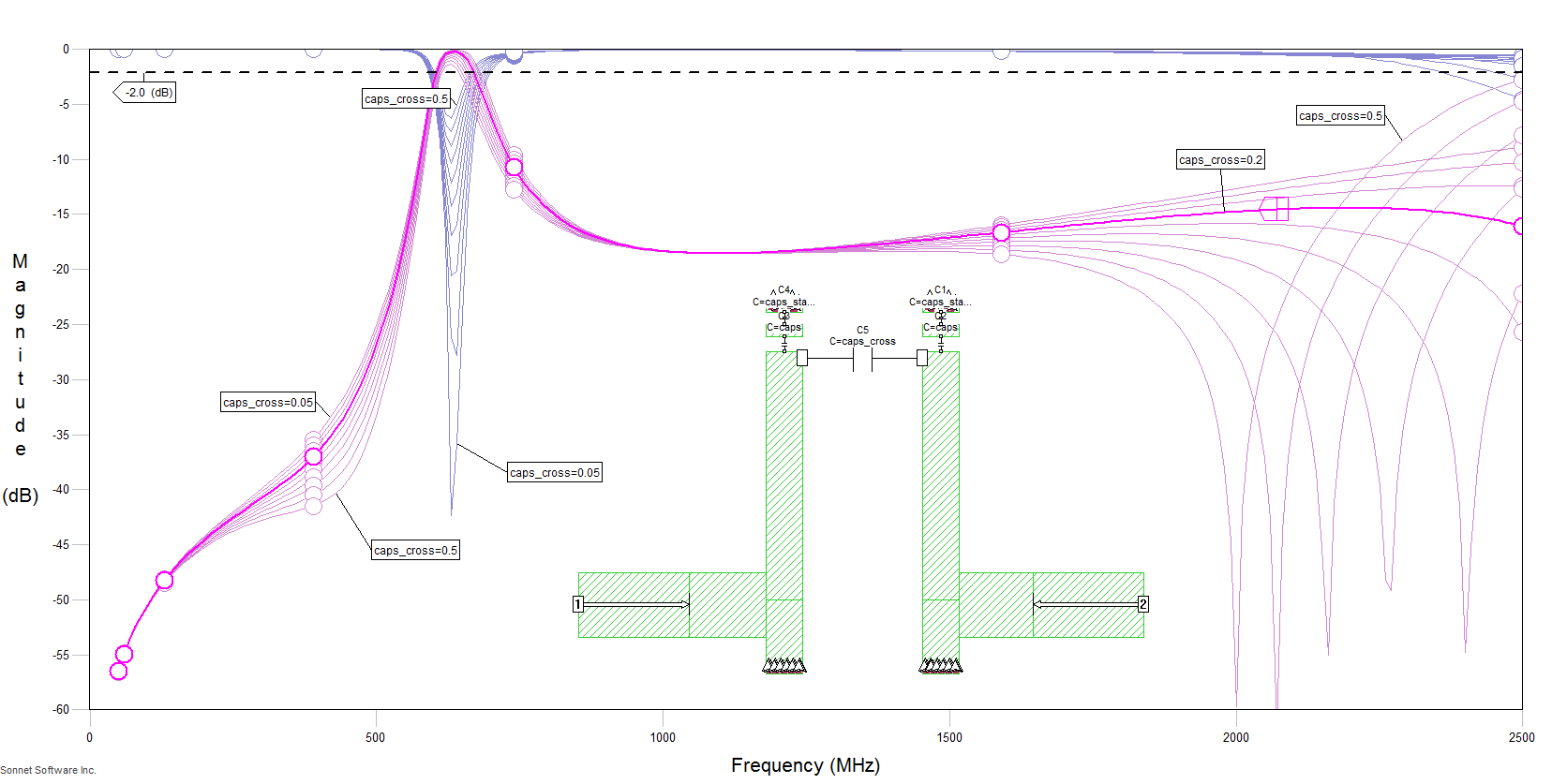
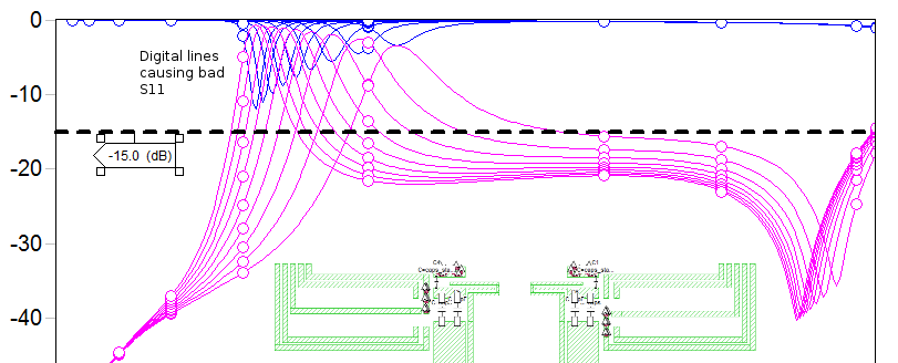
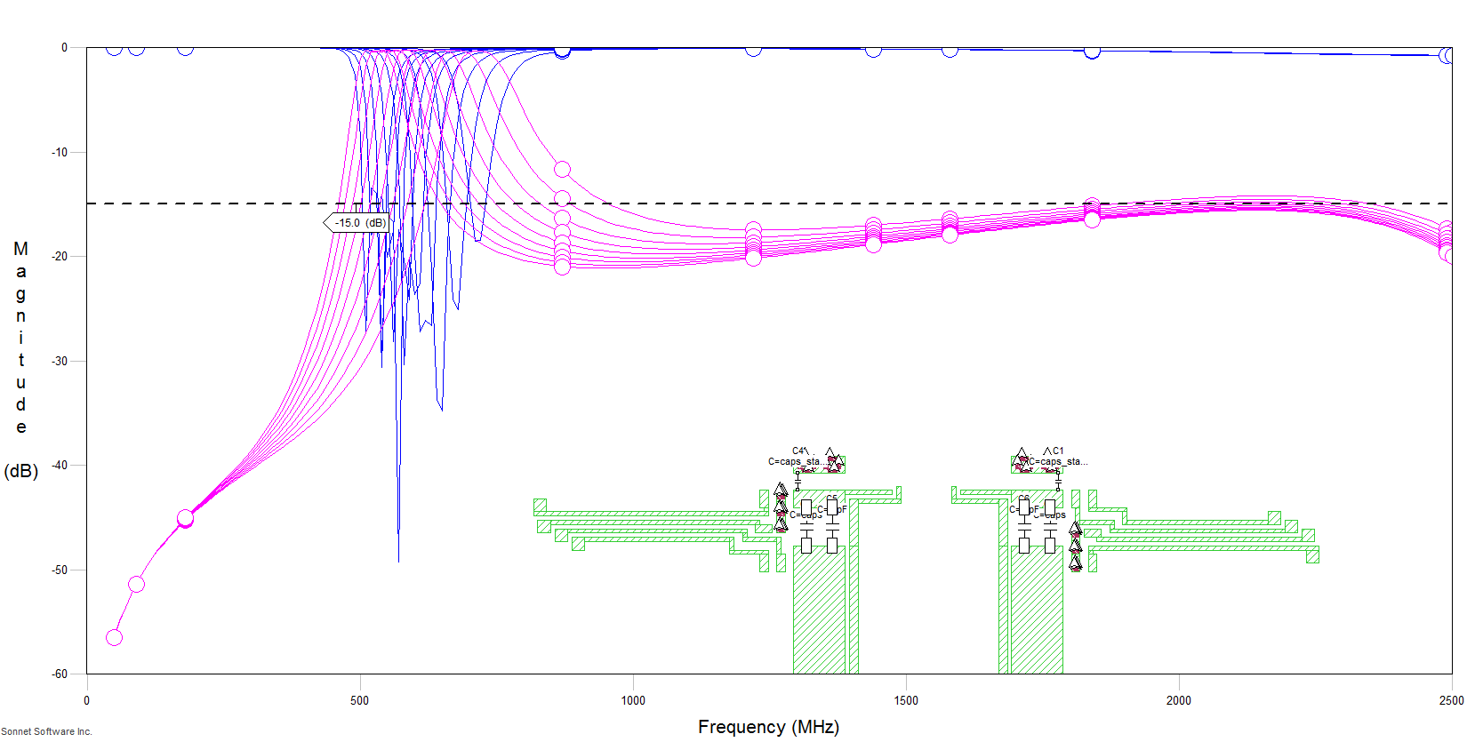
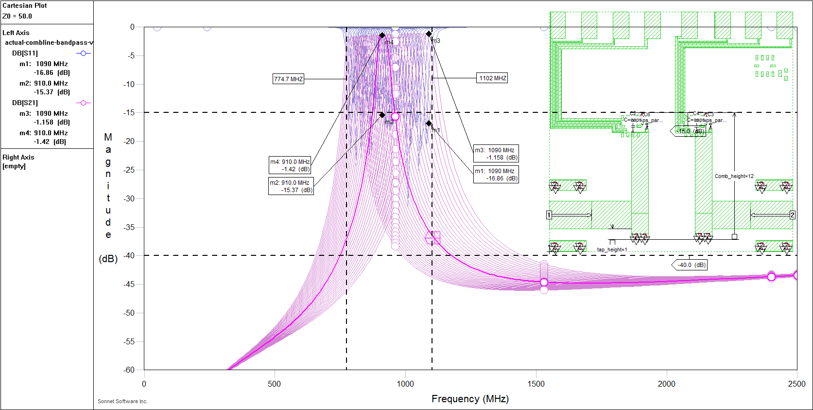
This simple interdigital pcb cap helped even more, finally pushing entire upper stopband down unde -15 dB insertion loss over the entire span to 2500 MHz and handily, putting the zero right on the middle of the 2.4 GHz wifi bands. With the final pin spacing below nothing changes. But it might when I add the long lines out.
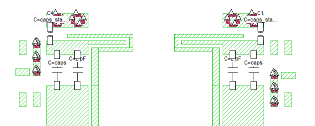
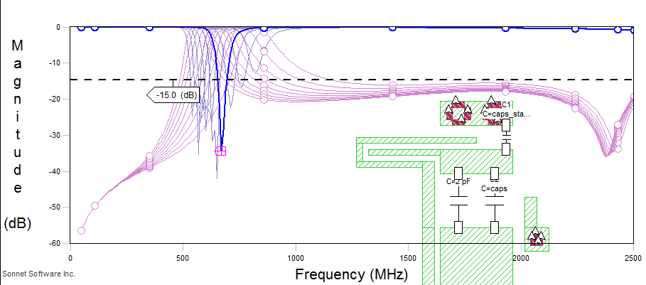
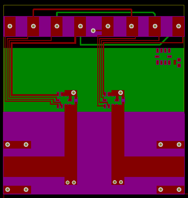
When I started adding the digital control lines it really threw the design out of wack. It's so small to start that the control lines were adding large parasitic effects. I noticed that they were acting like capacitance to the top of the combline and shifting the zero down and the S11 up, bad and good. So I redesigned them to minimize this effect *and* removed part of the capacitance I'd added to the cross-coupling H. This brought things back into line.
But with the better routing and smaller widths the result is even better than *before* adding the digital control + voltage lines. It's a good thing I figured out what caused the zero on the upper side to move back and forth before trying to route these lines. I might have given up rather than known how to control the effect (and use it).
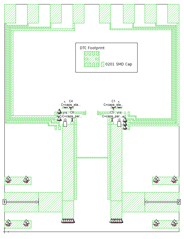
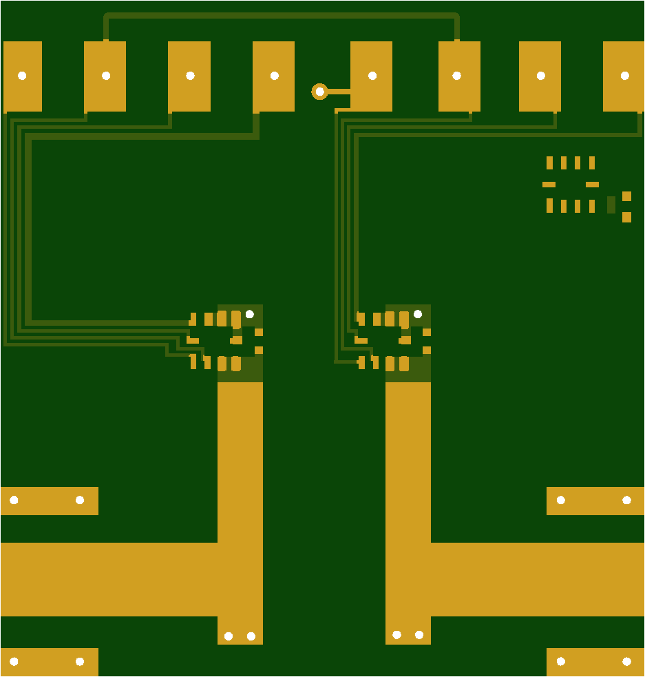
Looking just at the diagrams it may seem like there are no problems. But this is zoomed way in with 0.125mm grid size. The entire circuit is only 2.3*1.6 cm large. It's a postage stamp. So hooking up the SDA/SCL/SEN and voltage pins to those 0.5*0.5mm pads on the sides will not be trivial. It may be that I'll have to route them all to a header designed for directly hooking the esp8266 pins to fit up into, sort of like an esp8266 shield.
The capacitors are going to have to be tiny/dust size. I've never worked with SMD that small before. It should be interesting.

vs.
Since the actual scale is so small I wanted to space the digital control (and power) pins out as much I could. Doing this up far from the combline elements didn't have any effect on the performance. Neither did adding SMA ground pads for the end launch coaxial connectors.
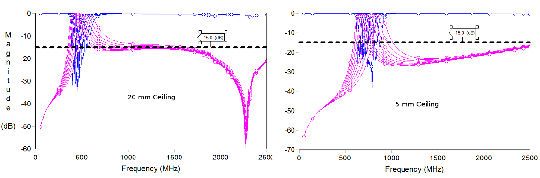
By default I set all my ceiling heights for the metal box the sim assumes to 10mm tall. Decreasing that to 5mm cause the S21 peaks to drop from the very good -0.25 dB to -0.5 dB and the S21 upper stopband to marginally improve. Increasing the height to 20mm caused the S21 peaks to raise to -0.16 dB while also increasing the depth of the upper passband zero.
But as the zero pulls down the other side of the curve inflects up and the width of the passband is inflated. That's not really desirable but it is what leads to the increased S21 performance, I think.
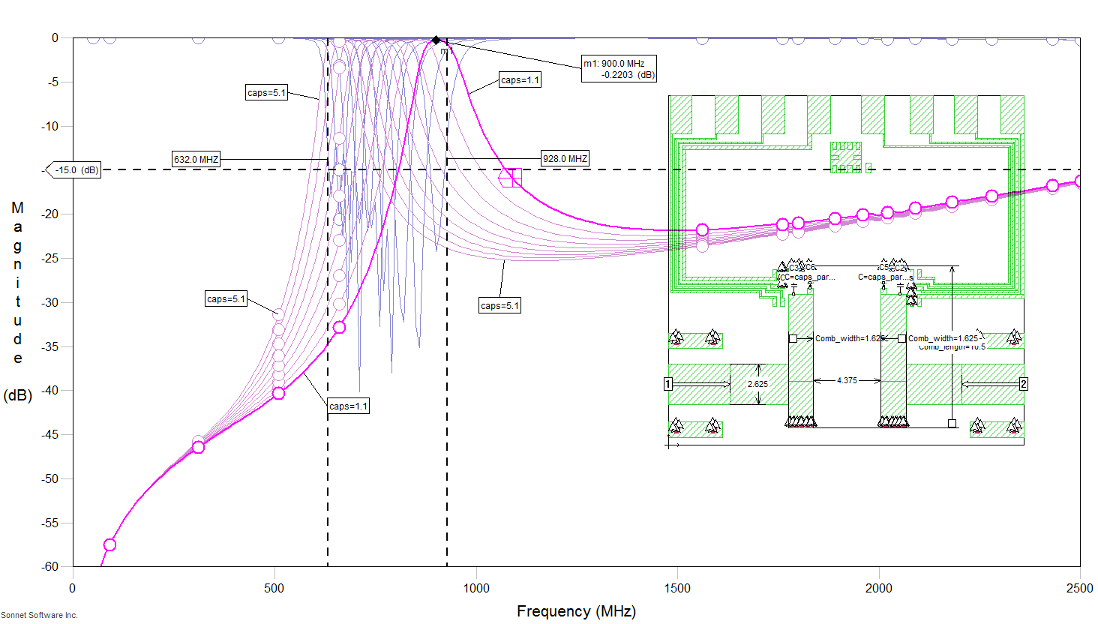
The way I split up the capacitance into two serial sections was an artifact of blindly copying the varactor design. With a DTC it's better just to have it span directly from the combline element to actual ground. By having the 30 pF cap in series the contribution of the DTC was marginalized and tuning range decreased even if the scattering parameters looked better.
But that means the DTC is now being used as a shunt to ground instead of in series. Instead of 0.6-4.6 pF it will have a range of 1.1-5.1 pF. In sims it makes a slight, useful difference.
Another surprising factor in weather the two peaks of the resonance split apart or contributed together was how far the PCB board and ground plane extend down beyond. This distance is fairly sensitive and slight (0.5mm) changes will change S11 by 10 dB. So that'll have to be carefully controlled when making the metal box itself.
It turns out, cheap PCB fab doesn't include really small vias. So I had to redesign everything for 0.5mm big vias.
Apparently, none, unless you're using the DTCs to shunt to ground, which I am. For that the RF- has to be be the set of pins going to ground. That means I can't just rotate the IC footprint. So that meant a bit of a redesign. But I think things turned out alright. It's going to be a pain to re-do the via and solder mask in kicad again though. I think I'll get both boards made and see if RF- polarity really matters as a test.
This lua code connects to to a hard coded wifi ssid then once it has an IP it connects to a TCP server running on a hardcoded IP and port. From there it waits for text instructions. On receiving anything in the form of a number from 0 to 31 it converts it to hex and sends it out the configured HSPI port to the digitally tunable capacitor.
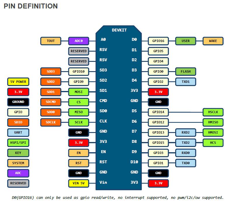
Normally GPIO15 (pin D8) is used as a SPI 'Chip Select' line. But this requires adding external resistors in order to not trigger some boot issue. Additionally people on the forums have reported HSPI CS not working with NodeMCU. So since the PE64904 only requires 3 wires I instead disable the HSPI CS (GPIO15/D8) and the HSPI MOSI (GPIO13/D7) by setting their mode back to normal GPIO. Then I use the HSPI MOSI pin as a GPIO and manually pull it low as a chip select command before spi.send() then manually set it high after.
For a server on the computer it connects to I use use netcat like,
nc -l 6005
and then type, say, 15 and hit enter. If it works it responds "ok".
15
ok
-- esp8266 mediated wifi:telnet control of PE64904 SPI based digitally tuned capacitor.

-- Config				esp12e		PE64904
-- -- Default HSPI for CLK and MISO
-- local CLK = 5           	 --> GPIO14 D5 | MISO, PIN 7 (SDA)
-- local MISO = 6            	 --> GPIO12 D6 | SCL,  PIN 5 (SCL)
-- -- Manual CS/SEN for chip select
local CS = 7              	 --> GPIO13 D7 | SEN,  PIN 6 (SEN)
local duration = 3000     --> 3 seconds
local i = 0
local result = 0

-- Turn on HSPI (dev 1) SPI at (80 MHz/8) 10 MHz
spi.setup(1, spi.MASTER, spi.CPOL_LOW, spi.CPHA_LOW, 8, 8)

-- Manual CS Pin (instead of HSPI CS)
gpio.mode(CS, gpio.OUTPUT)
gpio.write(CS, gpio.HIGH)

-- Need to disable HSPI CS D8/GPIO15 from being toggled.
-- Set pull-up to prevent potential issues.
-- ref: https://nodemcu.readthedocs.io/en/master/en/modules/spi/#spisetup
gpio.mode(8, gpio.INPUT, gpio.PULLUP)

function string.fromhex(str)
	return (str:gsub('..', function (cc)
		return string.char(tonumber(cc, 16))
	end))
end
function string.tohex(str)
	return (str:gsub('.', function (c)
		return string.format('%02X', string.byte(c))
	end))
end

-- Connect to wifi
print(wifi.sta.getip())
wifi.setmode(wifi.STATION)
wifi.sta.config("ssid","password")
print(wifi.sta.getip())

-- Connect to control server
local flagClientTcpConnected=false;
print("Start TCP Client");
tmr.alarm(3, 5000, 1, function()
	if flagClientTcpConnected==false then
		print("Trying to connect to server");
		local conn=net.createConnection(net.TCP, false)
		conn:connect(6005,"192.168.1.125");
		conn:on("connection",function(c)
			print("TCPClient:connected to server");
			flagClientTcpConnected = true;
		end)
		conn:on("disconnection",function(c)
			flagClientTcpConnected = false;
			conn=nil;
			collectgarbage();
        	end)
		conn:on("receive", function(conn, m)
			print("TCPClient:"..m);
			for i = 0,31 do
				if string==i then
					hexval = i.tohex()
					gpio.write(CS, gpio.LOW)      -->Activate the SPI chip
              				tmr.delay(1)                  -->1us Delay
					wrote = spi.send(1,hexval)    -->Write hex value
					gpio.write(CS,gpio.HIGH)      -->De-activate the SPI chip
					print("Started SPI DTC Control");
					conn:send("ok\r\n");
					tmr.delay(100)
				end
			end
		end)
	end
end)
For the init.lua file I use one I cribbed from the DoitCar demo from www.doit.am bbs.doit.am. Change "spiviaweb-nogpio15-v1.lua" to whatever matches.
--DoitCar Ctronl Demo
--sta mode
--Created @ 2015/05/14 by Doit Studio
--Modified: null
--http://www.doit.am/
--http://www.smartarduino.com/
--http://szdoit.taobao.com/
--bbs: bbs.doit.am
--

print("\n")
print("ESP8266 Started")

local exefile="sta"
local luaFile = {exefile..".lua","spiviaweb-nogpio15-v1.lua"}
for i, f in ipairs(luaFile) do
	if file.open(f) then
      file.close()
      print("Compile File:"..f)
      node.compile(f)
	  print("Remove File:"..f)
      file.remove(f)
	end
 end

if file.open(exefile..".lc") then
	dofile(exefile..".lc")
else
	print(exefile..".lc not exist")
end
exefile=nil;luaFile = nil
collectgarbage()